This thread has been locked.

If you have a related question, please click the "Ask a related question" button in the top right corner. The newly created question will be automatically linked to this question.

THS4631: Problems when applying THS4631 in a simple integrator circuit

Part Number: THS4631
Other Parts Discussed in Thread: OPA860, OPA615, LM7171

Dear TI expert,

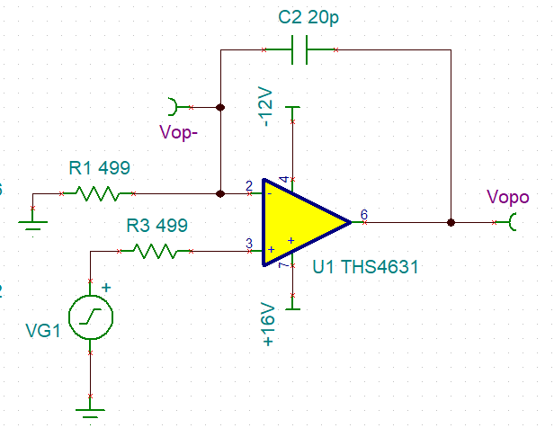
I design a PCB in which a THS4631-based integrator is used. The circuit is as Fig1. The power supply for 4631 is +16V and -12V, feedback capacitor C2 is 20pF, R1 is 499 ohms.

My goal is clear, and that is to control the output voltage’s slope by changing VG1 (“+” terminal voltage). The slope can be expressed by dVout/dt=VG1/(R1*C2).

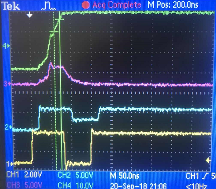
I do a test, in which VG1 is stepped from -1V to +5V. And the waveform is as Fig2, where blue waveform is VG1, red one is voltage at op amp’s “-” terminal and green one is the output voltage Vout. As you can see, after VG1 reaches +5V, it takes “-” terminal and output voltage 30ns to slowly reaches their target: “-” terminal voltage stables at one value and Vout rises at constant gradient. I have 2 questions.

  1. Why the response is so slow? 30ns is a bit long for THS4631, whose gain-bandwidth product is 210MHz. And why the “-” terminal voltage is about 80% of VG1?The big difference can lead to errors in the slope control.
  2. Is there any way to narrow the response time(30 ns here) and to eliminate or predict the voltage difference between THS4631 two input nodes?


Fig1

Fig2

Best Regards

Yatao

  • Hi Yatao,

    this is a slew rate issue. With a slew rate of 900V/µs a 30V output step takes 33ns.

    Kai
  • Hi Kai,
    But the Vout(green wavefirm) in Fig2 rises only 16V in 30ns, not 30V as you said.

    And why in this application the op amp's "-" node voltage  is always lower than "+" node's and their difference is not small(- voltage is 20% or even 40% smaller).

    Can you please ask my second problem in my post?

    regards
    Yatao

  • Hi Yatao,

    The slew rate will be less than 900V/us, since that is for a 10V step. Note that the slew rate is only 550V/us for a 2V step. The difference between the op amp's input nodes is due to the slew rate limitation, and is very predictable mathematically. It is due to the output not being able to slew fast enough to maintain the virtual short ideal op amp assumption. To reduce this slew time, you must find an amplifier with a higher slew rate.

    Best regards,

    Sean
  • Hi Yatao,

    a fast integrator can be built by using the diamond transistor in the OPA860 or OPA615. You might want to have a look at this thread:

    e2e.ti.com/.../718099

    Kai
  • Hi Sean,
    I now know that the "-" node voltage's large delay is due to the slew rate limitation. And the larger the slew rate, the smaller the delay.
    However, you say the difference between THS4631's input nodes is very predictable, which is confusing to me. Since the integrator circuit's R 499 ohms, CF 20pF, thus, a slew rate of 501.002V/us can create virtual short and such a slew rate should be easy for THS4631 to realize.

    I then try two things.

    1.I replace THS4631 with TI's largest slew rate voltage-feedback op amp LM7171 in TINA simulation and the difference between LM7171's input nodes is still obvious. 

    2. I lower the "+" node input voltage. And by the simulation, I find that the when "+" node voltage decreases, the "-" voltage also decreases and still is about 60% to 80% of + node voltage and never reaches virtual short.

    I gusee that when the input difference declines, the op amp's slew rate is also reduces. So, in my high output slope application, the input will always present a big difference.

    Can you show me how to calculate the difference or how to eliminate it?

    Regards
    Yatao

  • Hi Yatao,

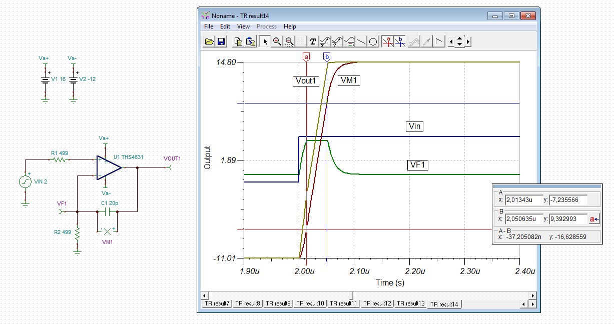
    see the following simulation of your circuit:

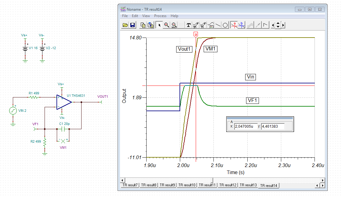
    Take care, the slew rate across C1 and the slew rate of the output of THS4631 are not the same. The slew rate across C1 can be calculated as 16.63V / 37.2ns = 447V / µs. This makes a current flow through C1 of 20pF x 447V / µs = 8.94mA. This results in a voltage drop across R2 of 8.94mA x 499R = 4.46V:

    yatao.TSC

    Kai

  • Hi Kai,
    You're right, and the waveforms you give are correct.

    In your first waveform, between cursor a and cursor b, the slope of Vout and VF1 equals. Outside the scope, their slope differ.


    But I think I haven't made myself clear.
    1. You give the input difference voltage by simulations. However, I just wonder how to calculate the difference voltage in theory just by THS4631's datasheet,not by simulation or experiments?
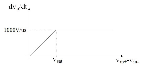
    2. Is there a graph or expression showing the relationship between input difference volatge and THS4631's output voltage slope? Like the figure below, noting that THS4631's largest slew rate is 1000V/us.


    regards
    Yatao