Because of the holidays, TI E2E™ design support forum responses will be delayed from Dec. 25 through Jan. 2. Thank you for your patience.

This thread has been locked.

If you have a related question, please click the "Ask a related question" button in the top right corner. The newly created question will be automatically linked to this question.

INA231: Schematic and programming of INA231

Part Number: INA231
Other Parts Discussed in Thread: INA220,

Hi team,

My customer want to use the INA231 to replace the INA220.

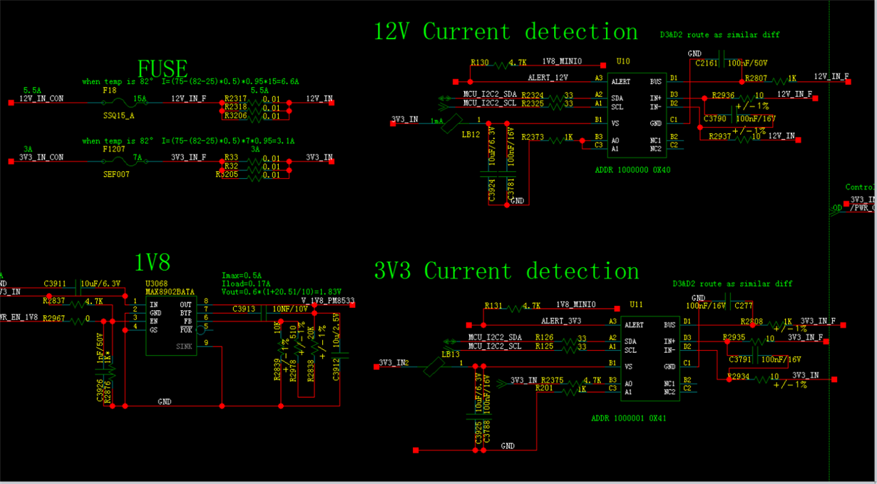
1. Please help to review the schematic of the INA231 as below:

2. For the programming, are the programming of  the INA231 compatible with the INA220? Are there so many change of the programming?

Lacey

Thanks a lot!

  • Hello Lacey,

    Thanks for using our forum.
    1. The sense voltage generated by the max current values 6.6A and 3.1A across the equivalent 3.33mohm shunts appear to be within the shunt voltage input specification, which is good. While the ALERT is pulled to a value lower than VS, the value is still considerably higher than the max VOL specification, so that should be fine. As for the input filter, this will contribute some gain and offset error to the measurement. Therefore if it is not absolutely necessary to filter out some high frequency component, your customer may consider removing that.

    2. INA220 and INA231 devices are similar in the fact that they utilize I2C for programming the configuration register and calibration register. However, the function of each bit within these registers does not match between these devices. The INA220 allows the user to have a different number of averages bus and shunt voltage measurements, while the INA231 does not. Another key difference is that the INA231 has a mask/enable register while the INA220 does not.
  • Hi Patrick,

    Thanks so much for your support!

    Can you also help to review the PCB layout from customer.

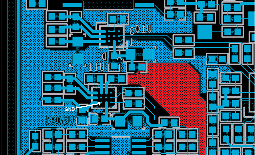
    Please help to look at the layout of customer.

    because customer's board is so complicated, there are so many layers, and they will put the trace in middle layer so need the via.

    Does the VIA affect much of the INA231?

    I notice the datasheet mentioned the input pin layout is so important, can the input trace go through the VIA?

    Please help to comment your concern for the layout.

    Lacey

    Thanks a lot

  • Hello Lacey,

    I made some adjustments to the pcb layout you posted above for the purpose of clarification.  Please let me know if the following is correct.  I made the gnd planes blue and the 3V3 plane red.  If this is correct, why do I not see a trace connecting the device ground to the ground plane?

    Aside from that, I think running the load trace between ground planes is not a problem.  There may be a little bit of parasitic leakage from the load line, but that should be really small. Also I think the inductance and resistance added by the via should be negligible.

  • Hi Patrick,

    Thanks so much for your support!

    For the GND connection, I need to double confirm with customer because there are so many layer maybe the blue one is not the GND.

    So double confirm with you, except for the GND, there is no other concern with the layout and pcb, right?

    Lacey

    Thanks a lot!

  • Hello Lacey,

    Yes I do not see any other possible issues with the layout. However, I did realize I overlooked one thing on your schematic originally. I noticed there is a 1k between the bus pin and IN+. This creates a voltage divider with the internal input resistance found at the Bus pin. The impedance has a 15% tolerance, yet in worst case it will still be relatively large compared to the 1k. However, I just wanted to alert to the fact it will introduce some additional error into your customer's measurement.