Because of the holidays, TI E2E™ design support forum responses will be delayed from Dec. 25 through Jan. 2. Thank you for your patience.

This thread has been locked.

If you have a related question, please click the "Ask a related question" button in the top right corner. The newly created question will be automatically linked to this question.

LM124AQML-SP: Power Sequencing

Expert 3821 points
Part Number: LM124AQML-SP
Other Parts Discussed in Thread: LM124, LM7800

I am using the LM124AQML-SP for signal condition before going into another buffer op amp that will drive a 12 bit SAR adc. My positive rail will come one before my negative rail and I found the below E2E post on power sequencing for op amps. Will the TVS diodes and silicon rectifier diode configuration described in the post mitigate any errors of my power sequencing? 

If I don't add these diodes, will my output go high until the negative rail is powered up? 

http://e2e.ti.com/support/amplifiers/f/14/t/801609?OPA548-a-Is-the-part-sensitive-to-power-supply-sequencing

  • Hello Jack,

    The diodes recommend are selfish. This means the diodes are there to protect the op amp from the application. The other post also forgot about the protection for the inputs. The diode do not protect the application from the output being high when a low was desired.

    A well behaved negative power rail will never go more than 300 mV positive, at any time included any foreseeable (or unforeseeable) fault conditions. With a well behaved negative power rail the op amp can be considered running single supply during the positive supply rail power up. 

    If the negative power supply is not well behaved, then be sure that no pins goes below negative power supply. Otherwise the diodes will be needed.  Also never short any input to ground directly. Always add some resistance, 1k ohm is sufficient in most cases.

    Can you provide a waveform of this power up? Note: the LM124 always thinks of itself as being a single supply op amp, where all pin voltage are relative to op amp's GND pin. 

    For any new LM124 application, I suggest reading the application note for this device.

  • Hi Jack,

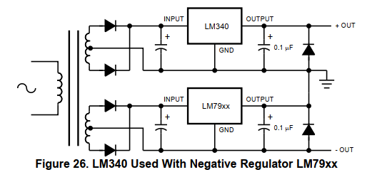
    voltage regulators providing a bipolar supply voltage can behave very strange during power-up and power-down, if unequal supply currents are drawn from the both supply voltages. This can make the positive supply voltage become negative or the negative supply voltage become positive, depending on which supply current is higher. This is dangerous not only for the OPAmp but also for the regulators because latch-up can occur. A good remedy is to clamp the output voltages of regulators by the help of a 3A Schottky diode each. Figure 26 from the datasheet of LM7800 shows what I mean:

    Kai

  • Hello Kai and Ronald, 

    Will the op amp still be damaged if there is no signal on the input pins before both rails turn on even if they turn on at different times?  

    If there is a positive signal or negative signal on the input pins before the positive and negative rail is powered on will that damage the op amp? 

    Also will I have to add diodes on my input as well? From the design guidelines, it appears that they already have them internally? "All the input pins have a diode from the input to the device’s GND, or V–, pin. In dual supply applications, the GND pin will be negative." - page 27

    The positive voltage rail will be powered from a 5V rail getting stepped up to 10V by a charge pump (driven by MSP which is powered by the same 5V rail but has an LDO to step down to 3.3V) and then a shunt reference voltage will create a clean 5V rail . The negative voltage for the op amp supply will be produced by a inverting charge pump (driven by MSP). I don't currently have any waveforms, but I can work on getting those if they are necessary. 

    With my power setup, do I still need to clamping? 

    3566.+-5V to 5V Final.TSCBidirectional Current Sense +-2A V2.TSC

  • Jack,

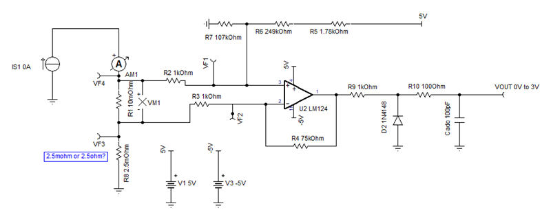
    I looked at the circuit. I'm hoping that R8 is supposed to be 2.5 milliohms instead of 2.5 ohms. Otherwise the input common mode range will be violated. Also the huge common mode swing will dominate over the desired sense resistor voltage for huge measurement errors with real 1% resistors..

    With a 5V supply, it best to limit required VOH to 3V. So I reduced gain to 75 and shifted offset to 1.5V, now +/-2A creates a 0V to 3V output for loads that are terminated to ground. I also reduce the op amp count to 1. Note the op amp input offset error of +/-2mV creates an output offset of +/-152mV (noise gain is 76)

    Low side Current Sense +-2A.TSC