This thread has been locked.

If you have a related question, please click the "Ask a related question" button in the top right corner. The newly created question will be automatically linked to this question.

LM2904: Differential amplifier circuit to measure the high DC voltage

Part Number: LM2904
Other Parts Discussed in Thread: , , LMV358

Hello,

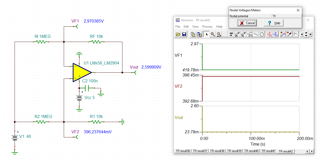
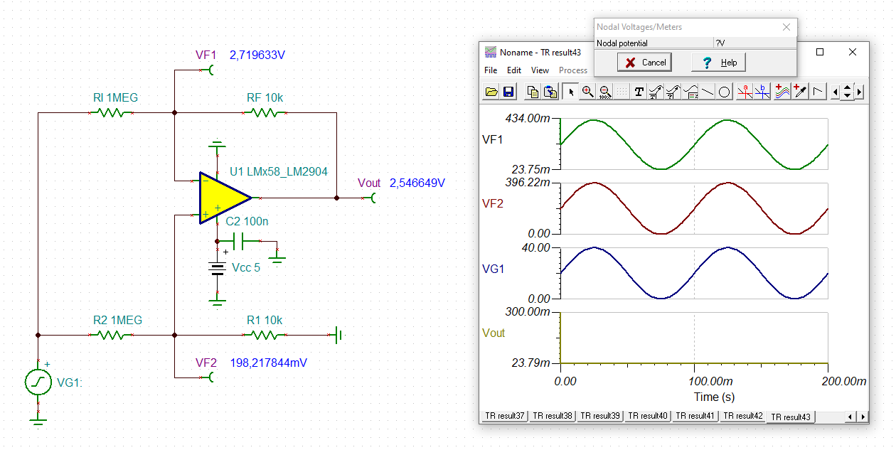
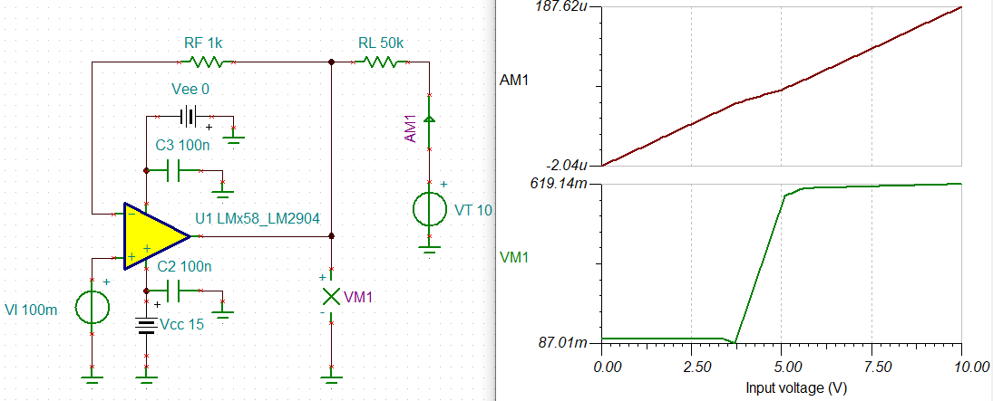
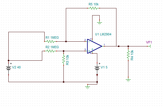
I'm using LM2904 to make a differential amplifier circuit to measure the high DC voltage(200Vdc~300Vdc). The circuit is shown as below:

This circuit works well, but when a common voltage is added to the differential input(eg. ~40V), the output of LM2904 will go higher(>500mV).  3pcs of PCB have the same test results.

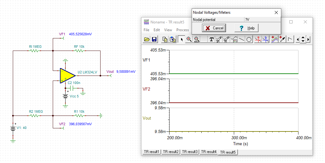
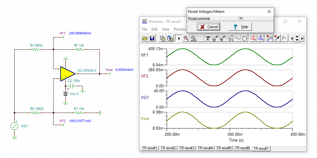
But if the LM2904 on board(soldered by production factory) is changed to LM2904B(which is the sample from TI), the common voltage added to the input will NOT influence the output of LM2904B.

Does that mean the LM2904 on board was broken during production?  or which parameter of LM2904B is better than LM2904?  thanks!

  • Former Member
    0 Former Member

    Hello TXH,

    Thank you for your question and welcome to the forum!

    First may I ask you, where is the high DC voltage being applied?  Depending on your application and whether there are very high DC common mode voltages, an isolation amplifier may be a good idea for your application.

    Can you share a little more information regarding your test?  What was the output voltage typically.  What was the final output voltage?  Any types of scope shots would also help.

    I would not expect the output voltage to change by that large of an amount.  Given that you are gaining down the input signal by 1/100, that your input signals should be nearly identical, and that you are using a difference amplifier, it is difficult to see how you could get such a large change in output voltage.

    How did you test the LM2904B?  Your answers will help me to debug your issue.

    Regards,

    Daniel Miller

  • Hi Txh,

    we need a full schematic of your circuit. What exactly are the input signals? Can you post scope plots?

    Kai

  • Hi Daniel,

    hhm, I think there's an issue with the new model of LM2904:

    lm2904_new_modelTSC.TSC

    Kai

  • Kai,

    The newer model tries to replicate complex LM2904 behaviour such as the two sink source and the crossover time delay. However it occasionally get stuck in an incorrect mode. 

    THX,

    For real parts exceeding 500mV output with high input common mode is actually a sink driver effect as the output must sink the R5 feedback current. Once this current exceeds roughly 40uA the output sink driver 'switches' to the PNP follower that has about 600mV of headroom requirement. For LM2904B the switch happens above 50uA (closer to 100uA).  This is effect is described in detail in the application note.  

    Because supply is 5V, try LM2904LV instead. It has a drain output sink driver so it won't have the >500mV issue.

  • Former Member
    0 Former Member in reply to Ron Michallick

    Ron,

    Thanks for pointing this out.  I had forgotten about this output stage consideration.

    TXH,

    Please consider pages 9 and 10 of Ron's app note.

    Regards,

    Daniel

  • Hi Txh,

    again, we need a full schematic of your circuit. What exactly are the input signals? Can you post scope plots?

    Kai

  • Hello Ron,

    Thanks for your reply. I tried to use LMV358 instead, and this problem is resolved.

    One more question is: How can we reproduce this 500mV issue of LM2904 by simulation(TI-TINA)?

    Also many thanks to Kai,Daniel!!!

  • Former Member
    0 Former Member in reply to TXH

    Hello TXH,

    I am happy Ron was able to answer your question.

    I'm not sure that this aspect of the part is covered in the model and I suspect it is not.  However, Ron might know for sure. 

    If Ron cannot confirm, then I will consult with my team's primary simulation engineer.

    Regards,

    Daniel

  • Hi Daniel,

    I'm also looking forward to his response :-)

    Kai

  • THX,

    I see that it is my turn to respond. It is not easy to make the model show this. On the creation of the new model, I asked that the model output stage was split into three blocks. That didn't happen. All my output stage requests are in the model but not how I asked. So it works sometimes. 

    Here is the switch between NPN collector always on sink and the PNP emitter follower. Chart "input voltage" is supply VT voltage

    Run Analysis - DC Analysis - DC Transfer Characteristics.

    This.TSC

  • Thanks, Ron!

    Very interesting.

    Kai