This thread has been locked.

If you have a related question, please click the "Ask a related question" button in the top right corner. The newly created question will be automatically linked to this question.

LMH32401: Simulation of LMH32401 with TINA-TI and its compatibility with ADS8861

Part Number: LMH32401
Other Parts Discussed in Thread: TINA-TI, ADS8861, ADC12QJ1600, ADS8900B, ADS9224R, THS4551, ADS127L01, OPA857, ADS8881

First of all, please send me the most recent TINA-TI spice model for the device LMH32401.

Then please send me some basic results (curves) of simulations carried out with the TINA-TI software and which allow to assess the performance of the LMH32401 device. For example: if we put a unit step or a pulse at the input, what are the outputs? I ask this to be able to verify my strange results.

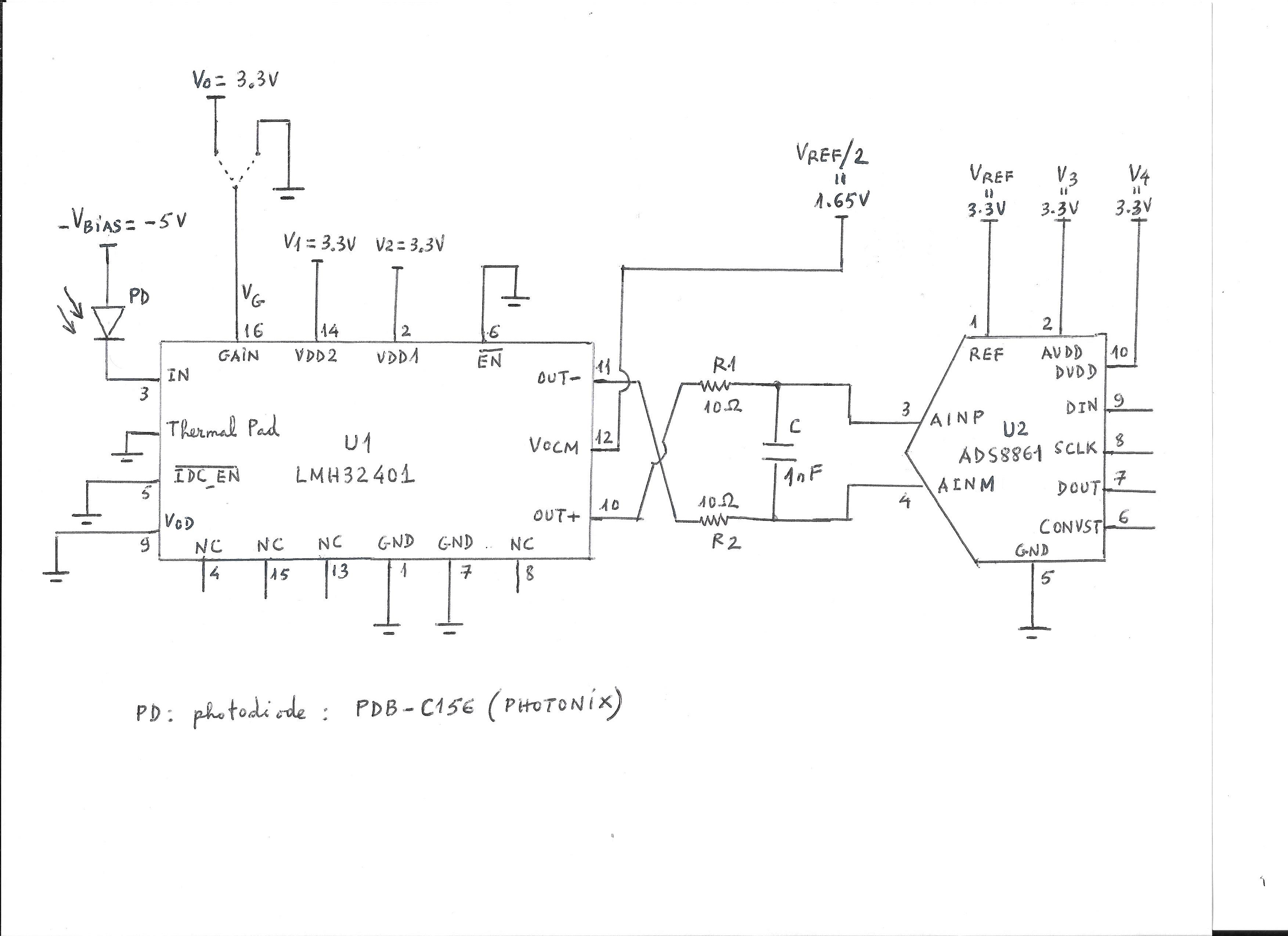
Finally, my design consists in detecting a light by a photodiode which I will place at the input of the LMH32401 device. At the output of the differential LMH32401 I will connect a differential ADC with SPI interface. Note that the ADC must be differential and also equivalent to a 100 Ohms load because the LMH32401 sis designed to drive at 100 Ohms load. Thank you for advising me an ADC who respect these conditions.

If you find that these two devices (LMH32401 and ADS8861) are incompatible, please offer me a differential TIA and a differential ADC with which I can realize my design. I prefer to use differential devices to minimize common mode noise.

  • Hello Andrianirina,

    The latest revision of the LMH32401 TINA-TI file is available on the product page of the device, and includes an AC response simulation within the file. I've added a picture of the transient simulation with a square wave and attached this TINA file below:

    3823.sbomb18b.TSC

    Note that the sampling rate for the ADS8861 is not fast enough to realize the full bandwidth of the LMH32401. Section 8.1 of LMH32401 datasheet recommends using the ADC12QJ1600 along with the LMH32401, I will add high-speed ADC team to see if they have any other recommendations. 

    In the meantime, can you help clarify your signal bandwidth and system requirements? Can you provide photodiode model or relevant specs?

    Also you've mentioned encountering issues with the LMH32401 model, can you provide screenshots and a copy of you simulation files with further details on the issues you are encountering?

    Best,

    Hasan Babiker

  • Hello Hasan,

    Thank you for your response which will certainly help me a lot.

    Thank you because I have received the latest revision of the LMH32401 TINA-TI file (3823.sbomb18b.TSC), as well as the results of an AC response simulation and an image of a transient simulation with a square wave.

    Thank you also for your remark concerning the ADS8861 compared to the LMH32401. I saw in the datasheet that TI recommends using an ADC12QJ1600 with the LMH32401, but my problem is that the ADC12QJ1600 does not have a SPI interface as my specifications require.

    I very much appreciate your decision to add a high speed ADC team to see if they have any other recommendations.

    For your information, my application concerns the medical world and for that I seek to develop an application to support the diagnosis of mental illnesses by detecting the biosignature obtained from the retinal signal. This new and unique application requires the design of a dedicated electroretinography device.

    I want to use 2 different photodiodes for the same circuit: the first for visible lights and the second for the broad spectrum (300 - 1100nm). I thought I would use the FDS100 for the broad spectrum light photodiode, and use the FESH0700 filter for visible lights, both manufactured by Thorlabs.

    Note that my choice for the LMH32401 is not yet stopped, nor indeed my choice for the photodiode and the anti-IR filter. I ask you to advise me of the materials (photodiode, filter, differential ATI to minimize the noise in common mode, and the differential ADC with SPI interface).

    Finally, the acquisition frequency is 100kHz minimum.

    Thank you for your help.

    Regards.

  • Hi Hasan,


    See attached the simulation file.


    I think I don’t understand how the LMH32401 device works and how the software works. Please help me by answering my questions below.


    Regarding the LMH32401 device, please explain to me the role of the Vocm pin. When should you give it a value, like you did in your simulation, and when should you leave it open?

    Likewise, in practice what are the values ​​to be given to the pins IDC_EN and VOD mentioned in the datasheet?


    See the attached file for the simulation I performed.Example_LMH32401.TSC

    When I do the DC analysis, is it normal that I get Vout + = Vout- = 1.1V, even if I change the gain (20kOhms to 2kOhms)?

    Please confirm that the results I get for the Transient Analysis, for both gains are correct.

    Please confirm that the results I get for the AC Transfer Characteristic are also correct.


    Thank you very much for your help.

  • Hello Andrianirina,

    • The Vocm pin helps determine the output common mode of the device. By default, if this pin is left open the output common-mode is set at 1.1V as you saw in your DC analysis. You can use the Vocm pin to change the output common-mode of the device if needed. 
    • As mentioned before you are getting 1.1V at the output since this is the default common-mode of the output. Note both Vout+ & Vout- are equal since you aren't providing an input a DC.
    • How you use the IDC_EN and VOD pins is up to you based off of how you would like to device to perform. I'd recommend going through sections 7.3.4 & 7.4.1 of the LMH32401 datasheet. Also you can directly see the filtering effect the IDC_EN pin has when performing an AC analysis in TINA with this feature enabled and disabled. 

    Best,

    Hasan Babiker

  • Dear Hasan,


    Thank you once again for your answer and your patience with me during your explanations.


    Why in your simulation and in mine, during the DC analysis I still have Vout + = Vout- = 1.1V even if I change the gain (2kOhms to 20kOhms)?


    I will read paragraphs 7.3.4 and 7.4.1 of the LMH32401 datasheet to better understand these IDC_EN and VOD pins.


    You wrote “As mentioned before you are getting 1.1V at the output since this is the default common-mode of the output. Note both Vout + & Vout- are equal since you aren't providing an input to a DC “. In this sentence, what do you mean by “you aren't providing an input to DC”?


    In the LMH32401 datasheet, it is written “The VOD pin is functional only when the LMH32401 device is used with a PD that sinks the photocurrent” and “The ALC mode only works when the PD is sinking the photocurrent”. What do these sentences mean? What is a PD which sink the photocurrent?


    Is my FDS100 photodiode manufactured by Thorlabs sinking a photocurrent?


    I will certainly have more questions for you, so I count on your usual cooperation. Thank you very much.

  • Dear Hasan,

    Thanks for your kind reply.

    I have read sections 7.3.4 and 7.4.1 of the datasheet but there are things that still escape me. So thank you to  answer my questions.

    As Vocm is set by default to 1.1V, ie when I leave this pin open, on which case we have to apply another voltage to it?

    Can I to connect the IDC_EN and VOD pins directly to the GND?

    How can I verify the gain (2kOhms or 20kOhms) by simulating the LMH32401 with TINA-TI using the LMH32401 model that you sent me?

    Finally, with a 100 Ohm resistor between Vout + and Vout-, what is the maximum current that I can inject at the input of LMH32401? I thought I could go up to 100mA (because of the 100mA-clamp), but a priori no.

    Always counting on your collaboration and your quick answer,

    Best Regards.

  • Hello Andrianirina,

    • You would need to set another voltage on the Vocm pin if you would like to alter the output-common mode level of the device. Typically differential ADCs have a recommended Vocm level that you will want to match, for the ADS8861 for example you will want to set this to Vref/2 to maximize the dynamic range. 
    • Yes setting IDC_EN & VOD pins directly to GND will set your offset at 0V & enable the DC cancellation feature
    • IG1 current is set to 0V at DC. Since there is not input being provided you will not be able to see the effects when u change the gain of the device. You can either provide a DC current into the circuit by adjusting IG1, or you can perform an AC analysis of the circuit. 
    • In regards to sinking of the photodiode, take a note of figure 7.2 of the datasheet. The anode of the photodiode is connected to a negative bias, while the cathode is connected to the input of the LMH32401, Because of this configuration, the LMH32401 will be providing the current to drive the photodiode. Like you mentioned this device has a 100mA clamp but realistically the output voltage will saturate at a much lower level.

    Best,

    Hasan Babiker

  • Hello,

    Take a look at the ADS9224R for one of our fastest SPI ADCs, or the ADS8900B for our most accurate 1MSPS product.  Both feature fully differential inputs.

  • Dear Hasan,

    I thank you once again for your answer which really helps me a lot.

    What's the downside if ADC's dynamic range is not maximized?
    Please let me know in the ADC8861 datasheet which part recommends setting to Vref / 2 to maximize dynamic range.
    When you say Vref, is that ADC8861 pin 1? As Vref = 4.5V for month, should I therefore apply a 2.25V voltage to it?

    I will connect the IDC_EN and VOD pins directly to the GND.

    I did an AC analysis of the circuit (with a current pulse) and was able to verify the gains, reporting OUT_DIFF / 100Ohms. Is this the way we should be doing?
    For the other simulation, how will I be able to supply DC current in the circuit by adjusting IG1? Is it by adjusting DC level?

    From figure 7.2 of the LMH32401 datasheet on the first page as well, is it therefore recommended to orient the photodiode as it is drawn there, i.e. that the anode of the photodiode is connected to negative bias, while the cathode is connected to the input of LMH32401? If so, then normally the LMH32401 should be able to supply 100mA. Am I wrong?
    Otherwise, how will I be able to know the limit current at which this device will saturate? I ask this question because the answer to this question will dictate my choice of photodiode.

    Thank you and I beg you to respond quickly as I plan to work this weekend to finish.

    Best regards.

  • Hello Andrianirina,

    I'd highly recommend going through the following precision labs video on interfacing an FDA with a differential ADC:

    https://training.ti.com/ti-precision-labs-adcs-driving-sar-adc-fully-differential-amplifier?context=1139747-1140267-1128375-1139103-1128655

    You will want to maximize the range of your ADC to improve the SNR of your signal. There are two sides of this you will want to think about, from the ADC side and from FDA or in this case the LMH32401

    1) In the ADS8861 datasheet you will see that the typical value for the "Input common-mode range" is Vref/2. Some ADCs specify a specific common-mode value that is needed, this is not the case for this ADC however you will be losing performance if you were change the common-mode value in this case.  Setting the common-mode to Vref/2 will allow for each of the differential inputs to swing from 0 to VREF giving you a total range of 2*Vref (going from -Vref to Vref).

    Because your common-mode is at the halfway point you are able to utilize the entire range of the ADC. However, if you were to change the common-mode value of the ADC (let's say for example to Vref/4) you will have to reduce your differential swing or you will be trying to drive input from  -1/4 Vref to 3/4 Vref. -1/4 Vref is outside of the range of the ADC so you will be losing some of your signal.  

    2) From the side of the LMH32401, you need to think about what is the maximum voltage the device can output. Yes, the LMH32401 is able to provide up to 100mA to your photodiode but with a gain of 2-kohm you will be trying to drive an output of 0.1 A*2000 ohms = 200V. Realistically the LMH32401 can only output a voltage swing of 1.5 Vpp so you will be clipping much earlier. 

    There is also the same swing issue when it comes to determining the common-mode for this device. Each output of the device has a certain output range, so if the Vocm is not set at the halfway point of your output you will not be getting the full output range of the device. If this turns out to be a problem you can add another FDA stage after the LMH32401.

    In regards to your simulation, yes you can do this by adjusting the DC level. Just remember that the LMH32401 has an ambient light cancellation feature which filters out your DC, so you will have to turn off this feature on the device if you want a differential output in DC.

    Best,

    Hasan Babiker 

  • Hello Dear Hasan,

    I never stop thanking you for your help.

    I understand much better now, thanks to you!

    My design boils down to the attached figure and I ask you to please tell me if you approve of it, knowing that:

    • For the moment I have chosen as the photodiode that of PHOTONIX with P / N PDB-C156 and its bias voltage will be negative with - VBIAS = - 5V (to reduce its capacity and increase its bandwidth)
    • For the LMH32401: VDD1 = VDD2 = 3.3V. Is this correct given that I have chosen - VBIAS = - 5V? IDC_EN and VOD linked to GND. What will be the consequence of the fact that I connect VOD to GND? In addition VCOM = VREF / 2 = 1.65V, in accordance with the recommendation in the datasheet of ADS8861
    • I chose for the filter, in accordance with R1 = R2 = 10 Ohms and C = 1nF, in accordance with the recommendation in the datasheet of ADS8861
    • For ADS8861 VREF = 3.3V, AVDD = 3.3V and DVDD = 3.3V

    Thank you so much.

    Best regards.

  • Hello Andrianirina,

    While this design will work there are a few things you can do to help improve your signal range to get the best SNR possible:

    1) Utilize the VOD feature on the LMH32401. Without this you are essentially halfing the total output range of the device. Please read section 7.3.4 of the LMH32401 datasheet and use equation 1 to calculate for optimal Vod input to provide. Note that if you keep the Vod pin open, the device will provide 510mV to the Vod pin internally.

    2) From here you will need to decide if you are willing to add a second FDA stage or not. To utilize the full range of your ADC, you will need to have Vocm set to Vref/2 (1.65V here) have a full differential output from -Vref to Vref. The problem here is that the LMH32401's differential output range isn't this high and to get the most out of your LMH32401 it is best to set the Vocm pin to 1.1V. 

    So if you are willing to add another stage, you can leave the Vocm pin of the LMH32401 open and add a device such as the THS4551 with its Vocm pin set to 1.65V to interface with the ADS8861. The THS4551 will be configured to gain the LMH32401 output so that you are achieving the full range of your ADC.

    3) If you would like to only use the LMH32401 and the ADS8861 I would recommend changing the Vocm pin on both to 1.1V. This way you aren't limiting the LMH32401 however you won't be getting the full range of the ADC. 

    Best,

    Hasan Babiker

  • Dear Hasan,

    Thank you for your email.

    Your explanations are clear and precise and I thank you for it.

    I am in the prototype phase so at first I will only use the LMH32401 and ADS8861. In this case, you recommend that I change the Vocm pin on both to 1.1V, so that I don't limit the LMH32401, but I won't get the full range of ADC.

    What do you mean by "change the Vocm pin on both to 1.1V"? What are you talking about "both" and what exactly should I do? Do I have to connect Vcom to a voltage of 1.1V even if according to the LMH32401 datasheet, if the Vocm pin open, Vocm is by default at 1.1V?

    You also say that in this case I will not get the full range of ADC. What will be the disadvantages then?

    Finally, can you recommend a photodiode that I can use for my application.

    Thank you very much and have a good new week.

    Best Regards.

  • Dear Hasan.

    I am coming back to you already.

    You also recommend that I use the VOD function on the LMH32401 because without it I will essentially reduce the device's total output range to half. If so, I will have less precision or what are the disadvantages?

    The best solution will therefore be to apply a voltage to the VOD terminal, but I have a problem with equation 1 in section 7.3.4 of the LMH32401 datasheet:


    with:
    • VOD = voltage applied to pin 9
    • VOD = (VOUT– - VOUT +)
    • RL = external load resistance

    If I am not mistaken, this equation can be simplified as follows: Vod = 1.2 x VPD x (1 / 20). Am I right?

    Then, I do not know RL because with the 10 résist resistors after the LMH32401 I have the ADS8861. So I don't know the equivalent RL resistance.

    Do I have to fix Vod first and calculate VOD? If so, how should I choose Vod?
    Or should I fix VOD and calculate Vod? If so, how should I choose VOD?

    Since the light I will detect will vary, so the current absorbed by the photodiode will vary too, do I have to change VOD each time?

    You write to me that if I leave the Vod pin open, the device will supply 510mV to the Vod pin internally. What will be the consequence and / or disadvantage?

    Can I connect the VOD pin to GND? If so, what will be the consequence and / or disadvantage?

    Finally, if I am going to use the LMH32401 and the ADS8861, which values ​​do you recommend to apply to VOCM (open, 0 or 1.1V?) And to VOD (open, 0 or what value?)? Why can't I apply 1.65V on VCOM?

    Looking forward to your response today and thanking you for your kind help,

    Best regards.

    PS: Could I know which country you are in? My personal email address is a.rktmll@gmail.com

  • Hello Andrianirina,

    • Yes you can just leave the Vocm pin of the LMH32401 pin open. Please Ignore my statement on "both."
    • By not using the full range of the ADC you aren't getting the full resolution of the device. You will be using fewer ADC codes to represent your signal.
    • You can use the input structure of in ADC datasheet to get an idea of your load (figure 47). So with two 96-ohm resistors, two 10-ohm resistors and two internal 10-ohm resistors you have a total differential load of 232-ohms. 
    • No you do not need to keep changing VOD, you would design for the maximum expected output to try and keep the signal balanced. Also the equation you posted doesn't seem to have come out right so I can't confirm its validity. 
    • Setting VOD to GND will half the output generated from the LMH32401. I would recommend leaving it open or set to a higher value if you are expecting to generate a higher output. 
    • In regards to a photodiode recommendation this is up to you based on your design requirements. In regards to narrowing down your choices based off the knowledge that you will be using the LMH32401, note that the device will begin clipping past 750uA and will work best when interfaced with a negatively biased photodiode.  

    Like I mentioned before the circuit you posted before will work, the recommendations i'm suggesting at this point is to try and help you get the best resolution possible. You can send me a direct message through the E2E forums if you'd like to take the conversation outside of this thread.

    Best,

    Hasan Babiker

  • Hello Dear Hasan,

    Thank you again for your clarifications.

    I believe we have done the tour for the LMH32401 and ADS8861 together. I will keep you posted if I have any further questions.

    Can you offer me a 24bits and 1MSPS or higher differential ADC, which can be installed with the LMH32401? Please also provide me with a connection diagram between the 2 devices.

    Thank you again.
    Best regards.

  • Hello Andrianirina,

    If your requirements are still limited by SPI, I would refer back to Collin's suggestions:

    "Take a look at the ADS9224R for one of our fastest SPI ADCs, or the ADS8900B for our most accurate 1MSPS product.  Both feature fully differential inputs."

    Best,

    Hasan Babiker

  • Hello Dear Hasan,

    Thank you for your propositions.

    Don't have 24-bit 1MSPS or higher differential ADC with SPI interface? I ask this question because your proposals are 16 and 20 bit.

    Thank you for your continued help.

    Best regards.

  • Hello Andrianirina,

    No the ADS8900B is the most accurate 1-MSPS SPI product. For 24-bit devices with SPI, the fastest seems to be the ADS127L01 which a 512ksps sampling speed.

    Best,

    Hasan Babiker

  • Dear Hasan,

    I come back to you to ask if I can fix VOD = 0.75V (voltage on pin 9 of LMH32401)? I ask this question because I do not know the equivalent impedance of the circuit (R, C) and of the ADC (ADS881), so I cannot use equation 1 on page 21 of the LMH32401 datasheet.

    I have other questions that I will ask you after.

    Best regards.

  • Hello Andrianirina,

    Yes you can fix VOD = 0.75V, it looks like there is an error on equation 1 of the datasheet where this should be RL + 20 on the denominator. This is because of the voltage division that will be occuring at the output with the internal 10-ohm resistors. Note that this does not only effect your VOD but your will divide your output as well. Note all specs in the datasheet are rated at a 100-ohm load, and with a larger load you will be able to achieve a swing greater than 1.5Vpp. 

    In summary, 0.75V fixed should work fine to achieve the maximum swing from your photodiode. I would say the VOD voltage would only be a concern if you are adding another FDA stage after the LMH32401. This is because it would be best to balance your output swing and you can set VOD to whatever the peak output voltage will be from your photodiode (you will need to test photodiode in this case to figure this out).

    Best,

    Hasan Babiker

  • Dear Hasan,


    Thank you for your kind response.


    I will use a photodiode (PD) that sources the photocurrent because this device is imposed by our customer. It will be the DFS100 from THORLABS.


    But according to the section 7.3.4 of the datasheet of the LMH32401: the VOD pin is functional only when the LMH32401 device is used with a PD that sinks the photocurrent. Set VOD = 0 V when the LMH32401 device is interfaced with a PD that sources the photocurrent.

    Also, according to the section 7.4.1 of the same datasheet, The LMH32401 device has an integrated DC cancellation loop that cancels and voltage offsets from incidental ambient light. The ALC mode only works when the PD is sinking the photocurrent. The DC cancellation loop is enabled by setting IDC_EN low.


    So, because I will use a PD that sources the photocurrent, as show in the attached design (the circuit is given by PHOTOLAB), I will set VOD = 0 V and will connect the pin 5 (IDC_EN) to the GND. Am I right?


    What are the negative consequences in my application of the fact that VOD = 0 V and IDC_EN = 0 V? What are your recommendations, knowing that I must use this PD?


    Thank you again for your kind help.


    Best Regards.

  • Hello Andrianirina,

    The LMH32401 is designed for use with a sinking photodiode and you will have limited performance using a sourcing photodiode. For another integrated trans-impedance device for sourcing photodiode, you may want to look into the OPA857. Depending on your desired phase margin, you may want to add some feedback capacitance because of the high input capacitance of the FDS100.

    Best,

    Hasan Babiker

  • Hello Hasan,

    Thank you for your kind response and advice.

    I chose the LMH32401 because it is differential and allows me to minimize common mode noise.

    How can I minimize common mode noise with the OPA857? Which ADC will I be able to use with this TIA?

    Do you have any other TIA that I can use with the FDS100 potodiode?

    Best regards.

  • Hello Andrianirina,

    What do you mean by "common-mode noise" in this case?

    The noise from your photodiode will be converted to a differential signal since the LMH32401 is in a single-ended to differential configuration. If you were to have a differential input sensor, having a FDA would be useful as then the common-mode signals from the sensor would be minimized.

    How you use the OPA857 will depend on the ADC you decide to use. If you would like to stick to a differential-input ADC, you can add an FDA stage after the OPA857, or you can switch to a single-ended ADC device.

    Best,

    Hasan Babiker

  • I never stop thanking you dear Hasan for your response.

    I prefer to outline the purpose of my design to you, so that you can enlighten me a little more and tell me if what I've done so far can be a solution:

    • I have a light that I would like to turn into an SPI signal.
    • I will therefore capture this light with a photodiode.
    • The photodiode will transform the light into current which I will amplify by the differential TIA LMH32401.
    • Next I will transform the differential output voltage of LMH32401 into an SPI signal.

    I call common mode noise noise at power supplies and the like, but not noise at the photodiode.

    What are my advantages of using the LMH32401 differential TIA over using a non-differential TIA?

    In your opinion, has my design so far: a photodiode that sinks the photocurrent (but not with the FDS100 that sources a photocurrent), with the LMH32401 and the ADS8861 can do what I wish to do?

    Thanks always for your precious help.

  • Hello Andrianirina,

    • The main advantage of having a differential TIA such as the LMH32401 is the ability to interface with a differential ADC without having to add an extra FDA stage. Fully-differential amplifers also have the ability to have a larger output swing using lower supplies (using the Vod feature in the LMH32401). Depending on the ADC used you may have to add an FDA gain stage after the LMH32401 regardless to achieve the full range of the ADC. The LMH32401 also has an ambient light cancellation feature which isn't available in our other devices. 
    • In regards to noise due to power supplies, you can refer to the PSRR spec of a device.
    • You should be able to interface the LMH32401 along with the ADS8861 but will need an FDA gain stage to achieve the full range & SNR of the ADC. Not sure if you have any specific SNR requirements...

    Best,

    Hasan Babiker

  • Dear Hasan,

    Thank you for your answer and your explanations.

    I don't have a specific SNR requirement. Depending on the results obtained in this prototype, we will refine the specifications.

    So in conclusion, can you tell me this design will work?

    Best regards.

  • Hello Andrianirina,

    You may have to fine tune the design based off your specific requirements, I recommend getting everything working in simulation first. You can look through this series for guidance on how to design your charge-bucket filter for use with the ADS8881. But yes, the LMH32401 & ADS8881 can work together without an additional FDA if you aren't concerned about achieving the full performance of the ADC. 

    Best,

    Hasan Babiker

  • Dear Hasan,

    How to make a simulation of the assembly "photodiode - LMH32401 - ADS8861"? Does TI have a simulator for that?

    Best regards.

  • Hello Andrianirina,

    You can use TINA-TI for that. Please take a look at the video series I linked in my previous post. 

    It looks like there is a TINA model available for the ADS8861 so building the input structure is unnecessary.

    Best,

    Hasan Babiker