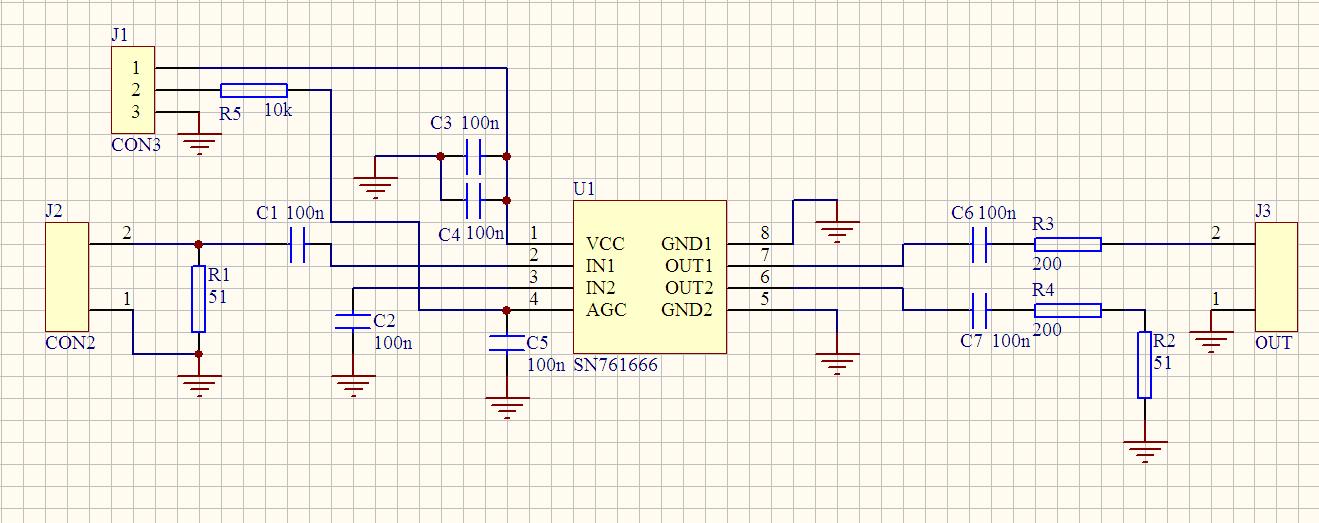
Can I use TL026 as an input amplification stage for a 10-bit ADC and use PWM with RC filter to generate the gain control signal? Thanks.

-
Ask a related question
What is a related question?A related question is a question created from another question. When the related question is created, it will be automatically linked to the original question.