Because of the Thanksgiving holiday in the U.S., TI E2E™ design support forum responses may be delayed from November 25 through December 2. Thank you for your patience.

This thread has been locked.

If you have a related question, please click the "Ask a related question" button in the top right corner. The newly created question will be automatically linked to this question.

Understanding this Precision Current Sink

Other Parts Discussed in Thread: OPA333

Hi:

I saw this precision current sink from this app note  :http://www.ti.com/sc/docs/psheets/abstract/apps/snla140a.htm (page 13) and i'm trying to understand its behavior.

What is re purpose of the NPN transistor. I understand the basic OPAMP + FET as a current source but what makes the addition of ths NPN a precision current source. if i understand the circuit right, the NPN will turn on once a current of 60uA or greater is sourced into the load , i.e assuming a Vbe of 0.6V, the NPN will be on for currents of (0.6V / 10K) or greater. Does this mean that for lower current levels, the NPN isn't linear or reliable?

I'm seekling a precision sink capable of sinking currents from 1uA to 5mA with an accuracy of 10nA or less. Will this circuit perfrom the task? I know the basic OPAMP+FET will not as its not linear for low currents.

Please anyone help if you can...

Also, i'm plannign to change Q1 to an N-channel MOSFET. Would that be ok as well?

Thanks!

David

  • Hello David,

    Do you have any particular questions or are you asking for a general overview of the operation?

    Basically the op-amp will use feedback to drive the output so that the voltage on the inverting input is equal to the voltage applied to the non-inverting input.  This is where the "virtual short" between the two inputs comes from.  If you look at the circuit, if the inverting and non-inverting terminals are equal then the "VIN" voltage appears at the node between R1 and R2 which is also shared with the collector of the NPN device.  Therefore the current through R1 will equal VIN / R1.  Since the majority of the current through R1 will be through the NPN of the device, the final transfer function is Io = VIN / R1.

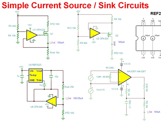
    This appears to be an older circuit and the Q1 and Q2 devices could be replaced with a common NMOS device now.  See a few more images below for other options:

    Regards,

    Collin Wells
    Precision Linear Applications

  • Collin:

    There is a reason why i'm asking how this circuit works. As i said earlier, i am looking for an ultra precision current sink that can deliver currents from 1uA to 5mA with 10nA (or better) accuracy. The current control would occur via a 16-20 bit DAC.

    I saw the circuit in an appnote and simulated it in LTSpice (from Linear Technologies) and it 'seems' to work (replacing the JFET with an N-channel FET) but i was miffed as to how it works. I need to know what properties the FET and NPN would need to have to make it work. I tried different N-FETs with different results. Some worked and some didn't.

    Yes, i do understand the basic principles of a current source/sink using an opamp+FET as i indicated earlier (and as shown in your first two graphics), but i was asking what does the additional NPN transistor add to the circuit to make it an ultra-precise current source, if it really is one.

    The standard opamp+FET works fine except for low currents under 100uA where it becomes non-linear as the FET begins to work in its non-linear region as it about to shut off, i believe.

    If you can suggest another circuit that would meet my specs, i'd appreciate it as well as i'm looking for an ultra-high impedance current sink.

    My application measures up to 256 resistors (via several muxes) valued from 0.01 ohms to 10K (using the 4-wire method) by injecting a known precise current and measuring the output voltage. This measured voltage will range from 0 to 5V maximum.

    Regards,

    David

  • Hi David,

    Sorry for the confusion, I actually didn't receive the second half of your message and only the first paragraph which is why I asked if there were any specific questions.  I guess there were several :)

    Let me dig in a little further and I'll reply back this afternoon.

    Regards,
    Collin Wells
    Precision Linear

  • Hi David,

    I took a closer look at the circuit and here's what I got:

    The main output current path of this current-sink circuit is through the emitter -> collector of the NPN.  But if you look at how the feedback voltage is developed across the "R1" resistor, the feedback voltage will include both the load current as well as any base currents.  Therefore in a normal NPN current sink, the current from the load would be off by the base current applied to the NPN.  This circuit solves this issue by sourcing the base current from the load through the JFET which will ensure that the current sank by the load is the same current that is delivered to the R1 resistor in the feedback network removing the errors caused by the base current in a standard NPN current sink.  This can be seen in the figure below.  Notice how the AM1 and AM2 currents are equal while the AM3 current is different than AM4 by the base current provided to the NPN.  The output is very linear down to low current levels which is shown in the image below the schematics.

    .  

    For the accuracy you're looking for I would suggest an low-offset, zero-drift chopper amplifier such as the OPA333 or similar.  If you choose to replace the JFET with an NMOS then be sure that it will operate in the low output current range required to source the base current to the NPN in low current output situations.

    Another high-precision current source option can be found on page 3 of the attachment below:
    2630.article3--edn-design_ieda_91803di_sep_2003.pdf

    Other current source/sink options can be found here:
    http://www.ti.com/lit/an/sboa046/sboa046.pdf

    http://www.ti.com/lit/an/sbva001/sbva001.pdf

    Please let me know if there are other questions.

    Regards,
    Collin Wells
    Precision Linear Applications


  • Collin:

    Thank you so much for the helpin explaining how this current source works. Can i have the TINA design files used in this simulation? That would be of great help. My eyes find it tough to read it off the screen :-)

    Also, as to the use of a MOSFET versus a JFET, I have to confess to you that i don't know the difference between the two devices. What is it about a JFET that makes it suitable for this application? I will be stepping or changing the current at a rate up to 20 KHz into loads up to 10Kohms. What propoerties of a JFEt should i look for to enable me to switch reliably and settle to 16bits or greater within 10 usecs?

    Is the value for R3 (10k) optimal?

    How do you calculate the output impedance of this current source?  ....  I apologize for these naive and/or simple questions.

    i just picked a MOSFET because my library from my cheap spice program only had MOSFETs and hardly any JFETs, none that i could source easily from vendors.


    Thanks,

    David

  • Hi David,

    You will find the TINA file attached below:
    2500.Precision Current Source_Compare.TSC

    Regarding the use of a MOSFET device instead of a JFET, the main reason that the N-JFET is used is that it is easier for a low-voltage op-amp to control the gate of the JFET to the appopriate level that closes the loop appropriately due to the smaller (and negative) threshold/pinch-off voltage in relation to the source voltage. 

    An N-channel JFET is a depletion-mode device where a negative decreasing Vgs voltage will turn off the channel from source to drain.  An NMOS is an enhancement device where an increasing Vgs voltage turns on the channel from source to drain.  Typical pinch-off voltages for JFETs are usually smaller than the threshold voltages (Vt) of a MOSFET.  The JFET shown in the circuit has a pinch-off voltage of only -0.65V.  Many NMOS devices have a Vt value over +4V, therefore with an NMOS in the circuit, the op-amp must be able to drive the gate at least 4V higher than the voltage the source is at.  In a 5V op-amp this will not leave much dynamic range on the amplifier output because the output will always have to be 4V above the source voltage which may not always be possible.  For example at higher output currents the source voltage of the NMOS will rise and load regulation will fail because the NMOS will simply not be able to turn on because the source voltage will be too high to allow the 5V op-amp to drive the Vgs voltage 4V higher than the source.  

    If you choose to use a higher supply voltage op-amp and choose an appropriate NMOS that will remain accurate in very low-current situations, which is required for the low-current modes, then your circuit should still work.  It will likely be easier to design this circuit with a JFET however.   It should be noted that negative supplies are required for the op-amp with the JFET circuit because the op-amp output voltage must go below GND in the very low-current operational modes.   

    Regarding your settling time requirement, the final settling time of the whole circuit will depend on the op-amp, JFET, and NMOS device as all of these devices are in the control loop that sets the current.  The op-amp will have an inherent settling time and the gate on the JFET will have to be charged and discharged by the op-amp output to drive the NPN appropriately.  My suggestion is that you get the SPICE models for all devices in your circuit and build/modify/test your circuit until you achieve the performance you're desiring.

    Regarding output impedance, instead of output impedance I'm assuming you're concerned with load regulation and the effect of different load impedances on the output current.  In this case, the "output impedance" or load regulation will be very good because the op-amp controls JFET and NPN through feedback to ensure that the load doesn't affect the output current.  Unless your load is very large and the current sink starts to experience compliance issues then the effect on a changing load impedance should be minimal.

    Regards,
    Collin Wells
    Precision Linear


  • Collin:

    Well said indeed!!! Thank you so much for your patient, concise and clear explanation for how the circuit works. I've even managed to understand the difference between a JFET and a MOSFET. I blieve, from your explanation, a JFET behaves like a normally closed switch that you have to apply power to open while a MOSFET behaves like a normally open switch that you need to power to activate or close the switch.

    Thanks also for answer on the load regulation for, as i said, my load is from 1 ohm to 10K and a maximum of 5V would appear across the load. I plan to use +/- 12V supplies for my opamp.  Yes, i will simulate with difference JFET types and see what happens.

    Now:

    1.  How accurate is your spice program, TINA compared to the real world? I'd like to trust it before i spin a board, which can be an expensive proposition, if TINA gives me false hopes

    2.  Secondly, does TINA accept other spice models from non-TI manufacturers?

    3.  My simulations from TINA show that the NPN is redundant, i.e hardly any meaningful current flows through it. Why is it used? I must be seriously missing something... I was using values close to what my circuit would be, such that VS up to 0.5v, R2 = 1.25K, R3 < 500 ohms and the load from 1ohm to 10K with V1 =  +5V ot produce a 2mA current maximum. I see that if R3 is increased, then the NPN comes in to play and carries the majority of the current, but the load current wouldnlt be equal to I(R2). Only if V1 is increased, then these currents would be equal as expected.

    I'm trying to understand the role of R3 and how to optimize it for my specific application.


    Thanks again for the help ...


    - David

  • Hi David,

    Glad it helped.  You're a little backwards on the JFET and MOSFET though.  A JFET is a depletion mode device, meaning when you apply "power" you deplete the channel and turn the device off.  A typical NMOS is an enhancement mode device, meaning when you apply "power" you enhance the channel and turn the device on.

    1.)  TINA will be as accurate as any SPICE program.  The accuracy of the SPICE simulation depends mostly on the accuracy of the component simulation models themselves.  TI spends a great deal of effort to produce very accurate SPICE models for all new linear integrated circuits.  Some of the older circuits may have models that are less accurate however.  A good practise is to open the simulation macromodels and check for notes which dictate which parameters are modelled and which are not.  You will need to check with the provided of any non-TI component simulation models to verify their accuracy. 

    2.)  Yes, TINA is a simulator like PSPICE, LTSPICE, TOPSPICE, etc.  It will accept any standard SPICE simulation models from TI or other manufacturers.

    3.)  Regarding the circuit operation, the resistor between the source of the JFET and the Emitter of the BJT will regulate which device sources the majority of the current.  In the circuit I sent you this resistor is "R3".  As the value of R3 is reduced more current will flow through the JFET, as R3 is increased more will flow through the BJT.  The exact value of R3 will somewhat depend on the JFET you choose, but I would suggest a value greater than 20kOhms to ensure most of the current flows through the BJT to avoid any saturation issues with the JFET at higher current levels.  The JFET will also take over operation at very low current levels and will source most of the current until the load current is increased to above around 25uA.

    I just ran a DC sweep and the current through R2 is equal to the current delivered to the load through the entire output current range you're desiring.  It seems that you're facing "compliance voltage" issues when you reduce V1 too far.  Basically if you design a circuit where the max resistance times current is greater than the supply voltage it simply can not work.  This is why when you increase V1 the circuit operates as expected.  Your voltage supply (V1) must be greater than the load current multiplied by the total load resistance which includes both the load resistance and the R2 resistance.   

     If you still have trouble getting the circuit to work, please attach it and I will take a look.

    Regards,
    Collin Wells
    Precision Linear Applications

  • Dear Collin Wells, maybe you can provide me some idea about my design since I believe you are the Guru in this problem. I’m designing a Functional electrical stimulator (FES) which required constant 200V to inject varying amplitude current pulse (e.g., 20 ~ 200mA). As you can see in figure 1, the constant voltage (i.e. 200 V) will inject the current thru the muscle and go to Q1. At the same time, the current (e.g., 200) produced through the bipolar junction transistor (MJE340) and sense resistor was equal to V5/ R23 . Basically, if I’m using constant resistor (R23) the current amplitude can be vary by changing the V5.

    But, I believe the implementation as above will not give a constant current when passing through the unstable muscle resistance. Hence, I want to combine the same idea as above but with additional of Wilson current mirror (i.e., which I assume will ensure the flow of desired current pulse amplitude) as shown in figure 2.

    So, I come out with an idea as shown in figure 3. Base on your knowledge, do you think this kind of design is practical?