


Other Parts Discussed in Thread: OPA4830
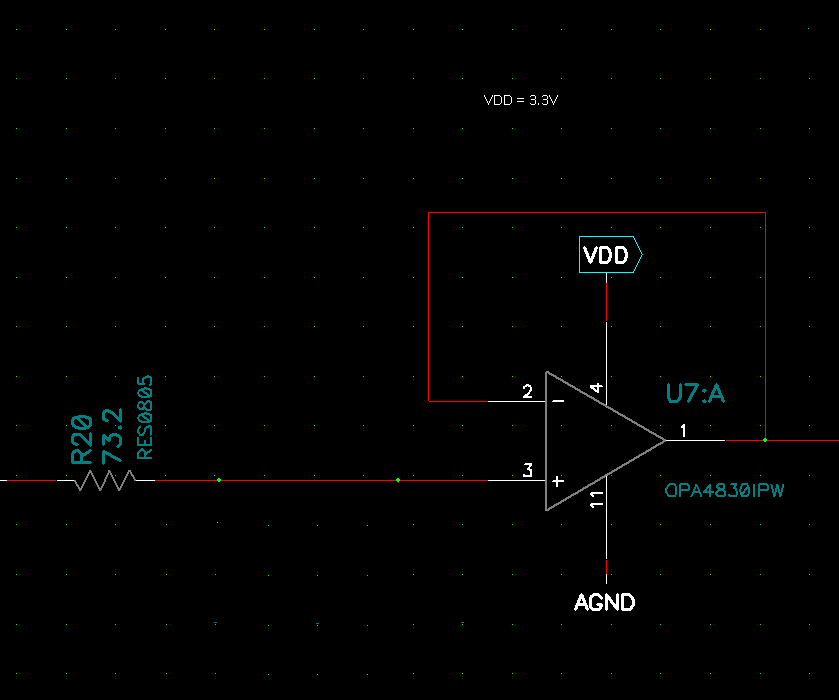
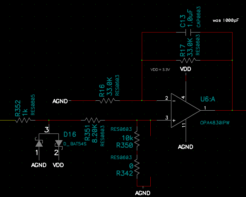
We have a problem with operational Amplifier OPA4830, was used two configurations and when we use it like a buffer happened a strange response in output. We did a test with same conditions third and fourth figure pictures in amplifier configuration it’s ok, but in buffer configuration output is not consistent (figs 1 and 2). Can I use this amplifier operational in buffer configuration?
Source +Vcc = 3.3V –Vcc = 0V;
Problem happened with configuration in first figure , not expected answer in second figure.
figs 1 and 2:


3 and 4 figs:
Output expected its ok.

Thanks.