This thread has been locked.

If you have a related question, please click the "Ask a related question" button in the top right corner. The newly created question will be automatically linked to this question.

Load Cell Circuit Design

Other Parts Discussed in Thread: TINA-TI, INA333, XTR106

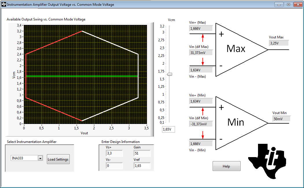
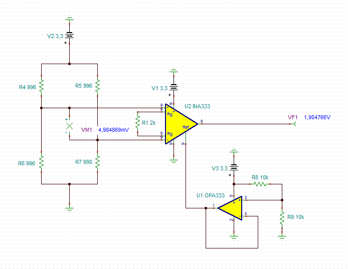
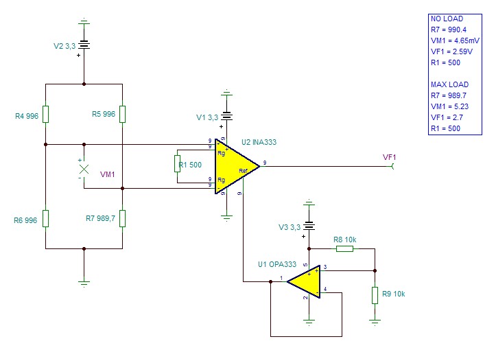
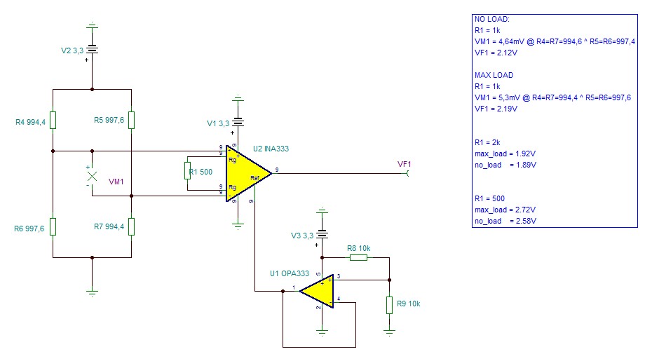
Hello to all! This is my first post here!

I need some help to design a circuit to acquire signals from two load cell sensors. I have looked for some TI instrumentional amplifiers, but i'm unable to chooise the rigth components for my purpose.

So, please, can someone indicate some TI components that is suitable for my project? 

  • Hi Furro,

    the load cell sensor and your application dictates the needed gain and the needed precision. With this in mind you start to design a suited circuit and to choose a suited OPAmp/INA.

    Kai
  • Hi Kai,
    I haven't a datasheet for the load cell, so I can't do many calculations using this sensors. They came out from recycled parts of some chinese domestic kitchen scales.

    I need that this sensors are able to measure force of max 1 N (or 1 Kg) with a resolution of about 1 g.

    The signals that came out of this sensors, should be in the range 0 - 3.3 V because my microcontroller ADC work with this range of voltage.

    I realize that for this circuit i need a power supply circuit, an INA and a output filter. For the power supply i have done a circuit using a ua7805 voltage regulator and using the adc specification, I have designed a low pass filter.

    I have some problem with the choise of the INA, so i have asked for some advice in this forum
  • Hi Furro,

    I would start with this scheme:

    Furro.TSC

    Kai

  • You might find this helpful too:

    Kai

  • Hi Kai,
    thanks you for the help. Now I study the circuit and the graph.
    A few thing about yours reply:
    1)The TSC file is for TINA simulator?
    2) How I obtain this graph and how I use and interpreted it?
  • Hi Furro,

    yes, the TSC file is for the TINA-TI simulator.

    The "TINA-TI simulator" and the "Vcm vs Vout Calculator for Instrumentation Amplifiers" can both be found here:

    www.ti.com/.../toolssoftware

    Kai
  • Ok, many thanks Kai, you help me a lot! ;)
  • Hi Furro,

    if your bridge is symmetrical, you should have a common mode input voltage of about 1.65V when powering the bridge with 3.3V.

    Can you measure the bridge resistance? This is the resistance from leg to leg. When the bridge resistance is high enough, you might not need R2 and R3 but can connect the bridge directly to the 3.3V supply.

    R1 was chosen for a gain of 101. Don't know whether this is suited for your application.

    U1 creates a reference voltage of about 105mV. From my last picture you can see that this makes sense when the bridge generates an unipolar signal, which is usually the case in a typical load cell application.

    Kai
  • Hi Kai, I'm sorry for the late answer.

    I have done some experiments for identify the load cells parameters.

    With a power supply of 3.31V I obtain this values: 1.66V and 1.65V from the signals legs to GND, and the voltage between the two signals legs it is 4.7 mV.

    For the other load cell I obtain the same values from the signals legs to GND (1.66V and 1.65V), while the voltage between the two signals legs it is 10.6 mV.

    The resistance from legs to legs it is 996 ohm and 993 ohm respectively.

    I have found some useful material in the TI site, in particular this reference design seem near to your advice. Now I also study this reference design.

    However, please, can you explain me how I can use the Vcm Vs Vout diagram? What is mean this diagram?

  • Hi Furro,

    the classical 3-OPAmp instrumentation amplifier has some restrictions. For a certain supply voltage and gain not all combinations of differential input voltage and common mode input voltage make sense. When powered from a single supply voltage, for instance, all combinations which would force internal nodes to go negative cannot be handled. Assume for instance that your common mode input voltage is not 1.65V but 1.0V, then your output voltage can never rise above 1.905V:

    Play a bit with this simulator and see how the minimum and maximum output voltage shown at the right side of picture will change.

    Yes, the reference design from Tim Claycomb is very good to start with.

    Another issue: The offset voltages you have observed, are these without any force? Or by other words: Is this the zero signal?

    Kai

  • Hi Kai, many thank for your patience!

    Today i have played with the TINA model but i have some problem to reproduce my load cell in the simulator.

    Using the resistor values that i have measured with my multimeter from one load cell, it's very difficult to obtain some working simulation.

    Seem that or my measure are wrong or the TINA load cell model is wrong. In any case i unable to reproduce correcly the load cell in simulation.

    Now i have found another reference design that show some formula and use a different TINA load cell model. I try to understand this example.

    Yes, the offset voltage of, respectively, 4.2mV and 10.6mV are the zero signal from my load cells. In the simulator I have problem with this voltage offset...

    In theory this voltage offset must be zero, but this isn't the case. Maybe are the load cell broken?

  • Hi Furro,

    as the bridge resistance of your bridge is rather high, I would omit R2 and R3 and give this scheme a try:

    A bridge offset can be simulated by a mismatch of bridge resistances:

    Check with this circuit whether you see any change at the output of INA333 when exerting a force to the bridge.

    Furro1.TSC

    Your link with the AC bridge excitation shows a much more complicate method to read the bridge. I wouldn't follow this approach at this moment. First check with the INA333 circuit from above whether the bridge is working at all. 

    Kai

  • Hi Kai,

    I have done some experiment using your model, in particular i have found the resistor value that give me the zero value and the max load value.

    2318.Furro1.TSC

    I have obtained the max load value using a 1 Kg mass on the load cell and measuring the voltage between the load cell terminal. This range is very narrow and it is only 0.5 mV. 

    With this range, the INA333 output change a bit from zero value to max load. This is a good behavior for this kind of circuit? My adc is a 14 bit one, i think that there is no problem to acquire this small voltage variation, but whit this load cell, i can obtain a better result in term of voltage range(a bit large voltage range from zero to max load)?

    I have a question about your model, you use only one resitor that act as strain gauge. Actually my load cell seem to have four strain gauge. I have done another simulator, like your, but with four variable resistors. However the result are the about same:

    MyFurro1.TSC

    It is correct this model?

    You have right about the ac bridge exci excitation reference design. I read it and it is a bit complicated for now. However there is some useful info about the load cell and also present a nice way to model the load cell.

  • Hi Furro,

    figure 1 of datasheet of XTR106 shows a way to adjust the offset voltage of a bridge. But I think that something is wrong with your load cell when the offset voltage of brigde is ten times higher than your full scale span (1kg). It should be just the opposite: The offset voltage should be much much smaller than the full scale span.

    In my simulation I use all four bridge resistances of the load cell (R4...R7). But to simulate the offset voltage I only changed R7 for convenience. The result is the same. But, of course, you are right, usually, all four bridge resistances will show a mismatch, not only one.

    Kai

  • Hi Kai,

    In the lab i have found another load cell and using a supply voltage of 3.3V, at no load, i measure 0.1mV between the signal terminals.

    However with a mass of 1Kg i measure a 0.5mV between the signal terminals.

    The difference between this two load cell are the presence of the offset at no load, in the first load cell there is an offeset of 4.2mV, while in the second load cell there is an offset of 0.1mV.

    However in both load cell, the max load value, respect to no load value, is nearly the same: 0.5mV in the first load cell and 0.4mV in the second load cell.

    I think that the problem is that I use a max load of 1Kg, but in reality both load cells are rated for 7Kg max, (that is the max value of the kitchen scale when the load cell are recycled).

    I haven't a mass of 7Kg so i can't verify this hypothesys with this load cells.

    However we have another kind of load cell. It is recycled from a jeweler scale of max load of 0.5Kg. In this case i measure, at no load, an offset of 10.6 mV, while at max load (0.5Kg), i measure a voltage of 14.8mV. In this case the difference between no load and max load it is in the order of mV, maybe is more normal respect the other two. I think that If this is normal is because i used a 0.5Kg for max load that is the max load of this load cell.

    I'm not an expert, so i can't give you an concrete answer about my hypothesys. It's difficult to found datas to compare my result. Maybe is better to buy a new cheap load cell and not recycle them from an kitchen scales... :)

  • Hi Furro,

    the offset voltage of a load cell is not per se a problem, provided the offset voltage is stable with time and temperature. When you analyze the signal of a load cell by the help of a microcontroller, then you do not even need a hardware offset adjust. You can easily adjust the offset voltage in your software.

    Another issue is hysteresis. How behaves the offset when you remove the weight again? Is there an hysteresis? A hysteresis cannot be adjusted by any measure. So, hysteresis might be the true limiting factor, not necessarily the offset.

    Kai

  • Hi Kai,

    at this moment i haven't saw any hysteresis effect on the load cell. It will come out when acquire some datas and I will analyze them. 

    My problem at this moment is the spam of the load cells. Actually this spam is very narrow and I think that this implies a poor resolution of the entire acquisition system.

    Two load cells have a spam of about 0.5mV between no load and max load, while the mini load cell have a spam of about 4.2mV between no load and max load.

    This will amplified from the INA333, however the adc will see a little voltage signal. I will need to choose correctly the gain of the INA333 for gain a maximum resolution.

    I think that with this sensors, is hard to increase their resolution.

    I agree with you about adjusting the offset voltage with the software because the entire system implies a little load that is always present on the load cell (It is a rotor with it's support, the total mass of they it's about 60/70 gramms).

    In any case I need to measure the tare and remove it from the final measurement.

    However I think that is better to use the hardware to remove the offset because i can choose an high amplified gain without saturate the INA333 output.