This thread has been locked.

If you have a related question, please click the "Ask a related question" button in the top right corner. The newly created question will be automatically linked to this question.

Percentage overshoot understanding?

Other Parts Discussed in Thread: OPA2197

Dear TI

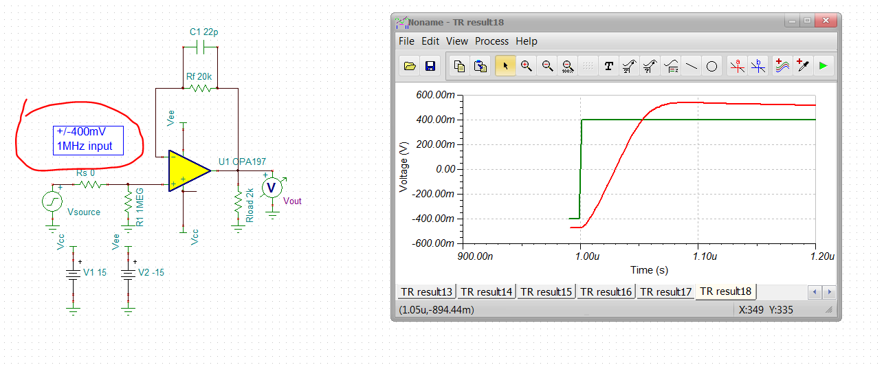
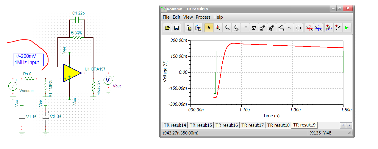
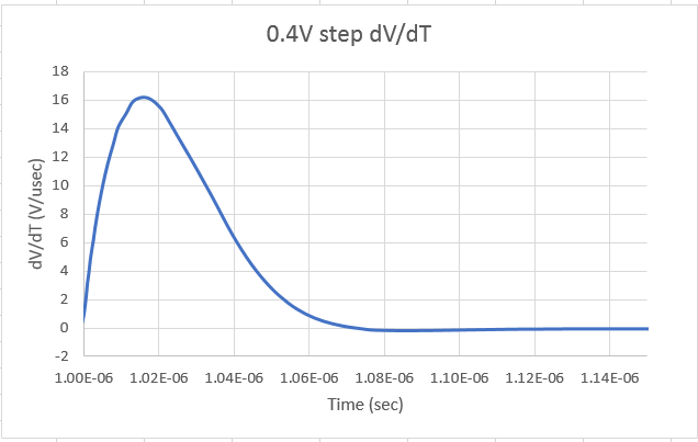
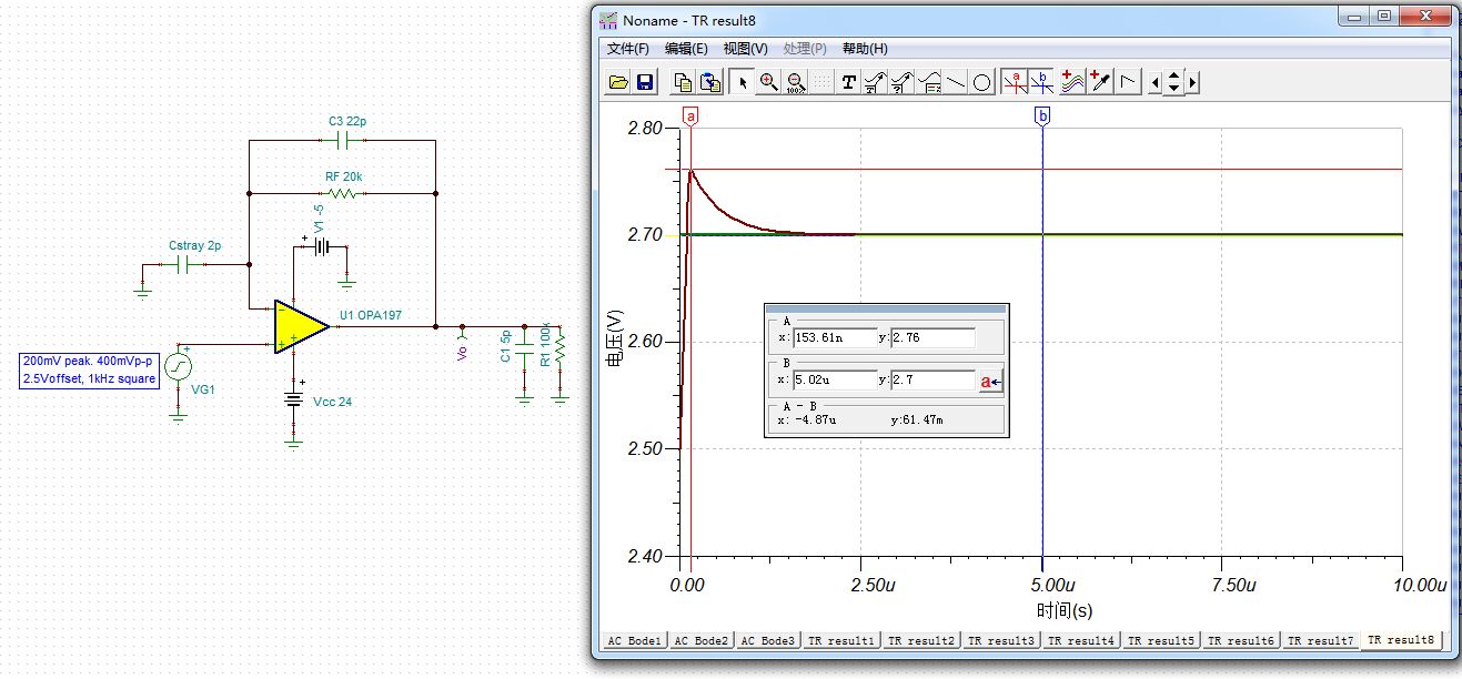
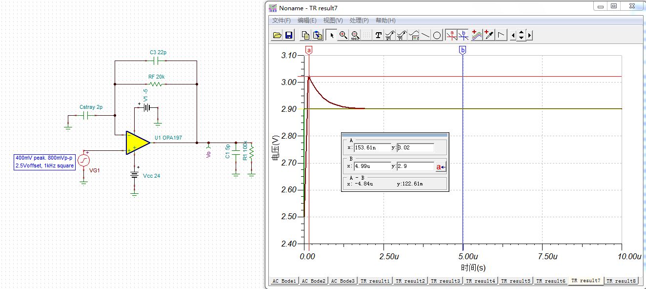
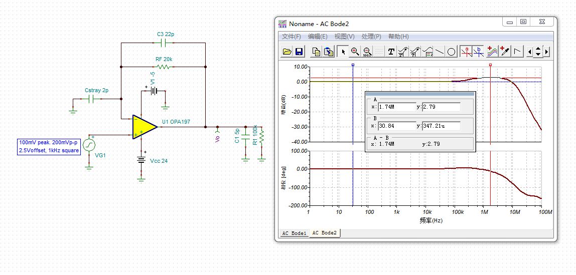
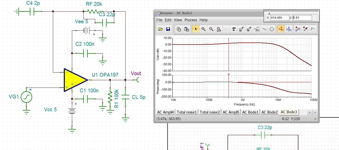
In TI doc op-amp stability (SLOA020A) page 13  figure8 - Phase margin and percentage overshoot versus Damping ratio,  team have disagreement about percentage overshoot definition in this figure, one view is that it should be " percentage of second overshoot peak to first overshoot peak" , another view is that it should be " percentage of first overshoot peak to final settled output value",   please advise which one is correct?

Thanks

Dennis

  • say you are trying to get a -1V to 1V step the the positive transition goes to a 1.2V peak on the edge, that is 10% overshoot, 0.2/2 =0.1. 

    You will have that overshoot on each edge if the input is fast enough on both. You can always slow the stimulus edge down to remove overshoot. 

    This discussion will show up in the next day or two in an article I will posting over on AnalogZone, but here is a useful plot relating dB peaking in the small signal peaking to % overshoot, 


    And then to target a particular +/-Vpeak on a square wave response with overshoot (OS, in 0.xx), solve this for +/- final values. 

    The article is mainly about how to determine if the transition will break off the ideal shape and go into slew limiting, but this part was necessary to set up a test sim. 

  • Hi Michael,

    Thanks for your replay, now it is clear to me, I will read your articles in next two days

    Thanks

    Dennis

  • You bet Dennis, that next article, The Signal Sped Up, Insight #15 has not quite posted, I will insert here when it does this week. The context of that one was making sure a 2nd order output step does not slip over into slew limiting on the transition. To illustrate that, I also had to work into the output Vpp including overshoot for a non-slew limited step to make sure it did not clip into the supply rails which is kind of what you are asking. 

    Slew limiting in the sim models is usually included, but does not necessarily pick up the actual response coming out of slew limiting. Physical devices normally show a small overshoot if slew limited then a non 2nd order shape recovery to final value. Also, physical devices extend their settling to final value if slew limited on the edge. That is almost never captured by sim models as we are asking them to pick up recovery from saturation or open elements internal to the device going in and out of slew limiting (the loop opens in that case). Best settling time will stay far away from a slew limited transition. Insight #16, if I work on it, will be on settling time issues. 

  • Hi Michael,

    Thank you for your help on this.

    -Tim Claycomb

  • Morning Dennis, 

    Yes, Planet Analog got this next one posted today on higher speed amplifier slew rate - Eq. 2 and 3 here generate that %os vs dB peaking curve - along with quite a number of other things covered here. 

    The LMP8671 I used to show a slew limited large signal step in simulation does not recover from slew rate like you would expect, but good enough for illustrating non-linear edge effects. The amount of overshoot of course had to be considered to avoid clipping into the supply rails in the example design. 

    https://www.planetanalog.com/separating-linear-from-slew-limited-performance-in-high-speed-amplifiers-part-2-of-2-the-signal-sped-up-insight-15/

  • Hi Michael,

    Thanks a lot for sharing, I am digesting the article, will ask you questions when I have

    By the way, I would like to ask a question about our recent op amp stability testing result, the test input signal is a 400mV peak 1KHz square wave, the circuit under test is a unit gain buffer using opa2197(there is 20K resister and 22pF cap in the feedback in parallel), the measured output result as below, it seems it has a fairly high first peak(no second peak), almost 200mV, which is  percentage overshoot 25%, corresponding to phase margin it is around 43deg, which is below than 45deg, can you give some analysis on the test result

    Thanks

    Dennis

  • Well Dennis, that is not a 2nd order shape with ringing, that is a slew limited shape with a single overshoot and recovery. 

  • Your input edge rate was very fast I suspect, try dropping the amplitude until you see ringing then the check the overshoot vs. phase margin. 

  • Well Dennis, this question is similar to what I was trying to do in that article.

    1. What is the closed loop SSBW, I get about 13.5MHz here. 

    2. Then what would your .8V step ask for for peak dV/dT - that would be approx. 2.85*0.8V*13.5Mhz = 31V/usec, exceeding the stated 20V/usec in the device. The sims show this, 

    3. To stay under that 20V/usec physical limit, try dropping your test amplitude to 400mV or +/-200mV step and see if a ringing step results. I cannot yet get that in sim for some reason, it just stays a single overshoot with decay, but that is the model, not the part. 

  • Well Dennis, I thought I had my issue, that 1kHz is too slow to get enough points on the edge for a good dV/dT. Partially right, but anyway - 

    1. going to 1MHz +/-400mV clearly shows that single overshoot with decay indicative of slew limited transition, 

    2. dumping that out and taking the dV/dT indeed shows a good 20V/usec flat region exposing the model slew rate is correct, 

    3. dropping that down to +/-200mV should have moved that below the peak dV/dT available to about 0.4*2.85*13.5Mhz = 15.4V/usec peak dV/dT. but it still does not ring like a 2nd order step would, 

    4. Dumping that out for dV/dT extract shows about the right peak dV/dT but no negative transition

    Looking at the SSBW, that is not really a 2nd order shape - looks more like a zero pole shape so these results might make sense. 

  • Hi Michael,

    Thanks for this input, I am wondering where the constant 2.85 from? (2.85*0.8V*13.5Mhz = 31V/usec)

    I did some simulations by myself it seems the result is not consistent with different Methods simulation, I was somehow confused, maybe there is something wrong with my simulation, please checkout the result.

    Method#1 small signal load step

    I run different step 100mV peak, 200mV peak and 400mV peak, they got the same result of first overshoot of 15% compared to settled voltage

    Method#2, AC sweep peaking, the peaking is around 2.79 dB, which can refer to a percentage overshoot of 27%

    Method#3, loop gain simulation AOL and 1/Bata to find phase margin, the result is pretty good, the phase margin is 70.51deg 

    Thanks

    Dennis

  • Quite a number of good questions there Dennis, 

    I did test your LG PM and also get 70deg so there should be no peaking in in the small signal response if it is indeed just a 2nd order response. 

    I had alluded earlier that it looks more like a zero plus those higher 2nd order poles giving that peaking. 

    So the short answer is the response shape is getting that overshoot since there is a zero in the the response shape, looking close at the SSBW that slight phase lead proves that before it is overridden by the 2 poles out around 10MHz, So a lot of what I was telling you does not directly apply due to this zero in the response for your set up. I don't have the peak dV/dt for that situation (or overshoot) easily available right now 

  • Hi Michael,

    Thank you for all the help on this question!

    -Tim Claycomb

  • Hi Michael,

    Appreciate for your help! you are right there is a zero caused by PCB stray cap on pin In- of op-amp  to adjacent plane or trace, when I put a small RC filter at the input In+ or increase the feedback to be 51pF, the first peak will decrease to be an acceptable level(peak overshoot percentage<10%)

    Thanks

    Dennis