This thread has been locked.

If you have a related question, please click the "Ask a related question" button in the top right corner. The newly created question will be automatically linked to this question.

OPA2335: How to avoid the EOS damage

Part Number: OPA2335
Other Parts Discussed in Thread: OPA335

Hi Team,

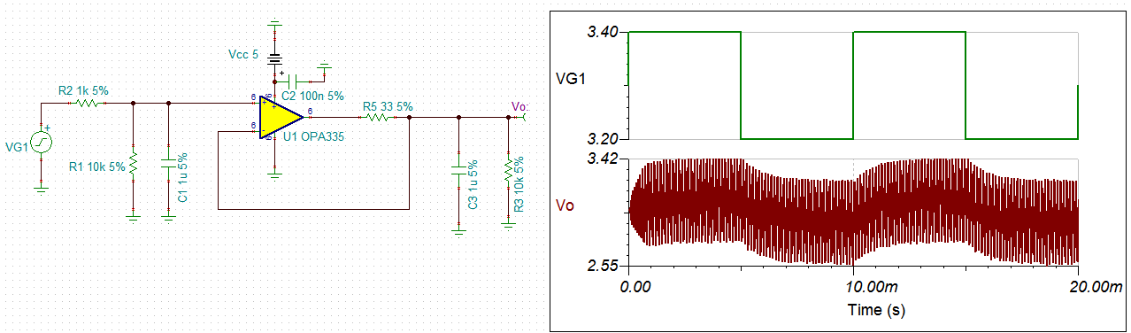
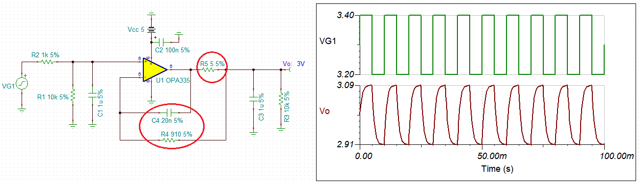
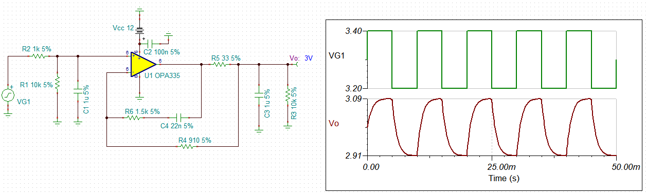
  My customer used OPA2335 which always reported EOS damage,  the OPA2335 Input is 3.3V, which used to generate 3V, and the 3V is used for ADC sensing clamp.  This is for UPS application.

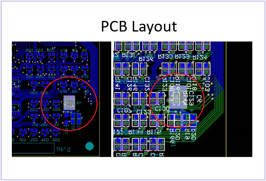
  Could you kindly review the schematic and PCB layout, and give comments on how the EOS come and how to avoid?  the schematic and PCB layout shown as attached file.

  Expect for your kindly reply, thanks.OPA2335 Issue.pptx

Best Regards

Benjamin

  • Hi Benjamin,

    the PCB layout of BAT54 section is not capable of handling ESD. You could try to separate the green and blue traces by an additional ground plane. But even the traces within the same plane are way too close to each other. So ESD will stray couple from one trace to the other without being affected by the BAT54. The traces within the same plane should be separated by ground fills which are connected to the ground planes by as many vias as possible.

    So best totally route the BAT54 section from scratch and try to avoid all the mistakes made earlier :-)

    Don't allow ESD to force their way so deep into the PCB. ESD must be shunted to ground right at the edge of PCB or even earlier on a separate PCB before reaching the main PCB. Have only filter caps on the main board and these right at the connectors. And have the BAT54 section way earlier.

    Kai

  • Hi Benjamin,

    I noticed that the OPA2335 reference circuit is unstable, and and it has no required phase margin in the close loop of the op amp circuit, see the simulation. 

    After some phase compensation in the circuit, I finalized the design as follows. With the modification, I am getting the unity Gain BW is measured at approx. 8.45kHz with phase margin of 75 degree. The 3.0V reference circuit is stable now. 

    /cfs-file/__key/communityserver-discussions-components-files/14/OPA2335-EOS-12072020.TSC

    My customer used OPA2335 which always reported EOS damage, ... the 3V is used for ADC sensing clamp.  This is for UPS application.

    Which part of OPA2335 IC are damaged frequently. I would like to know more about where the damages are likely occurred in the Op Amp and under what types of transient conditions, if it is known. Are there any visual damage pattern on the IC? Please let us know.

    Best,

    Raymond 

  • Hi Benjamin,

    If you want to retain the original circuit and add the compensation components in R6, C4 and R4, it will work just as good for stable 3V reference. The phase margin of the circuit is very stable. 

    Best,

    Raymond

  • Hi Kal,

      For the PCB layout, could you kindly share some simulation data or detailed description for how the ESD generated and how to along the trace into the OPA2335 side?   should it be helpful if add the filter for higher frequency& low frequency filter close to the VCC pin?

      Could you kindly point where is the BAT54 for the PCB layout? I double check the customer in the PCB layout file and couldn't find the BAT54;  

      Expect for your kindly reply, thanks.

    Best Regards

    Benjamin

  • Hi Raymond,

      For the stability,  what's your comments for the stability relationship with EOS/ESD damage? My understanding is even with the unstable situation, it shouldn't affect for the EOS/ESD for the VCC but only affect the performance of output, 

     Expect for your kindly reply, thanks.

    Best Regards

    Benjamin

  • Hi Benjamin,

    What's your comments for the stability relationship with EOS/ESD damage?

    You mentioned EOS damage in the initial inquiry. EOS is the exposure of a component or PCB to a current or voltage beyond OPA335's max. ratings. I would like to know if the damages (always as the initial query) are occurred at OPA335's input, output or elsewhere on the IC, before I can comment on it. 

    There are differences between EOS and ESD damages. ESD damage refers to rapid discharge of accumulated charge. You may have both issues on the  design and PCB. 

    Best,

    Raymond

  • Hi Raymond,

      The previous FA reports shown the PIN4 & PIN8 are shorten,  these 2Pins are voltage PIN. 

  • Hi Benjamin,

    we need way more details to be able to give help. How does the PCB look like? Where is ESD coupled into PCB? Has the PCB passed an official ESD testing?

    Kai

  • Hi Benjamin,

    As Kai pointed out, there are not enough details that we are able to hypothesize the what is going on at OPA2335 under EOS/ESD events. Can you describe the damage events or sequences of the part? Under what UPS operation or mode of operation,  the OPA2335 is likely to be damaged. Please send us the image of the damaged part as well. 

    Best,

    Raymond

  • Hi Kai, Raymond,

      I would close this loop and discuss on the mail, which give clearly understanding for more details.

    Best Regards

    Benjamin

  • Hi Kai,

      Could you kindly share your email address? or can you reach to me by my mail: benjamin-zhou@ti.com?

    Best Regards
    Benjamin

  • Hi Benjamin,

    Per your request, we are going to move the EOS/ESD discussions via internal email. I am going to close this inquiry. 

    Best,

    Raymond