This thread has been locked.

If you have a related question, please click the "Ask a related question" button in the top right corner. The newly created question will be automatically linked to this question.

INA826 with OPA333 - why use active integrator rather than passive high-pass?

Other Parts Discussed in Thread: OPA333, INA826, OPA314, OPA317, INA333, INA118, TINA-TI, INA332

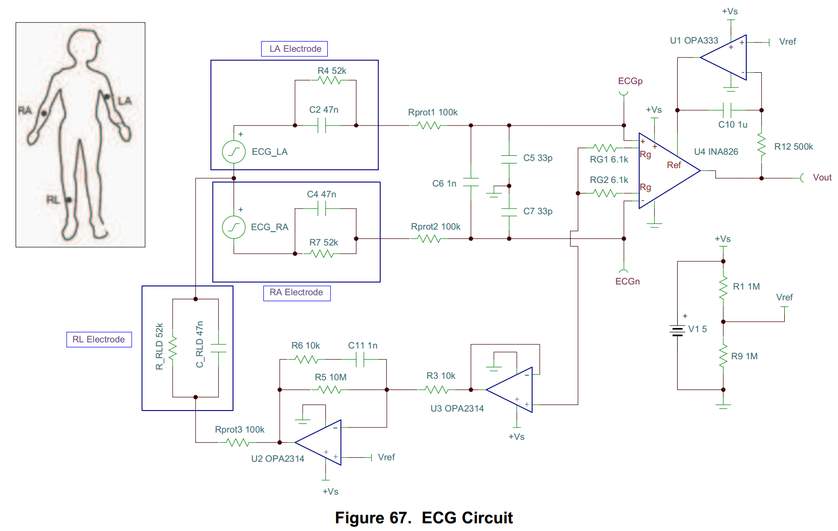
Looking at Fig 67 on p27 of the INA826 datasheet, there is a single-supply one-lead ECG circuit that uses OPA333 as an integrator to remove the DC component of the output signal, by inverting it and feeding it back to the reference input of INA826.  I have three questions:

A.1) What is the reason for using OPA333 (which is a relatively expensive op-amp), rather than simply a ground reference (or low-impedance rail-splitter if single-supply) and a passive high-pass filter (or even an active high-pass filter with a much cheaper op-amp, such as OPA314).  Does it somehow improve the input common-mode range, or cause an effective increase in the output voltage range?

A.2) What is the high-pass frequency for the circuit in Fig 67, and how do I calculate it?  Is the slope of the cut-off filter the same as a one-pole passive high-pass filter?  For diagnostic ECG it should be 0.05Hz; what combination of resistor and cap would be best for that?

A.3) What effect would there be on performance if I substituted a much cheaper op-amp, such as OPA314 in place of OPA333?

Second part:

B.1)  If I wanted to use input buffer op amps before the INA826 (e.g. OPA314 simply as a unity gain buffer) would this reduce the performance at all?  Could it improve it, by providing the INA826 all the bias current it could possibly require?

B.2)  In a unity-gain buffer, does the CMRR of the op-amp matter at all?  I have read in a published book that it is irrelevant in unity-gain, whilst an electronics engineer has told me it is still important.

Thanks!

  • Hello Bob432,

    I will do my best to answer as many of your questions as possible, but please understand that though we are familiar with ECG, it is only one of many applications that we try to support.

    The applications engineer who developed this circuit developed an accompanying presentation, which can be found here:

    e2e.ti.com/.../2437.ecg-heart-signal-acquisition

    Here are my responses:

    A.1) There are likely other op amps that you can use instead of the OPA333. However, I would still recommend an auto-zero op amp such as the OPA333 because it has no 1/f noise. A lower-cost amplifier that you could use is the OPA317. The topic of ac coupling vs. integrator is discussed in the aforementioned presentation on slides 35-37. In short ac coupling degrades the ac CMRR.

    A.2) The cutoff frequency of the integrator is 1/(2*pi*R12*C10)=0.32Hz. You would have to increase R12 and C10 appropriately to get a cutoff frequency of 0.05Hz.

    A.3) The noise would increase.

    B.1) The input stage of the INA826 is already made up of two high impedance non-inverting amplifiers. The only components between the INA826 and the electrodes are the protection resistors (which I assume are required). If anything, inserting op amp buffers will add error due to their respective offset voltages (which will be amplified by the IA) and add noise to the signals. So, I see no need for additional op amps in series with the inputs.

    B.2) CMRR is a measure of an op amps ability to reject common-mode signals. In a non-inverting configuration, the common-mode voltage is the same as the input voltage. Therefore, as the input signal changes, an offset voltage is induced at the input of the device (in addition to the initial input offset voltage). This offset voltage is then amplified by the device. For example, an op amp with CMRR of 80dB will have 100uV of input-referred CMRR induced offset for each 1V change in the input signal (relative to mid-supply). In a gain of 1V/V, this equates to 100uV at the output. In a gain of 100V/V, this equates to 10mV at the output.

    If the amplifier is in an inverting configuration, the common-mode is fixed at the voltage applied to the non-inverting terminal. If the applied voltage is mid-supply, there will be no input-referred CMRR induced offset. If the non-inverting input is connected to a voltage other than mid-supply, the CMRR induced offset voltage is calculated as shown previously. For example, given an op amp with a single 5V supply (2.5V is mid-supply), inverting configuration, 80dB CMRR, and ground-connected non-inverting terminal, the input-referred CMRR induced offset voltage is 2.5V*100uV/V=250uV. This offset will remain relatively constant with respect to the input signal, but will still be amplified by the gain of the device.

    With respect to common-mode voltage, you may find the TI Precision Labs video on Input and Output Limitations interesting (www.ti.com/.../precision-amplifier-precision-labs.page).

  • Thank you for taking time to give such clear answers - you certainly clarified a few things for me. However, my main question was why an integrator is used rather than tying the reference terminal of the INA to mid-supply and using a passive high-pass filter *after* the instrumentation amplifier to remove the DC offset from the output of the INA. (This is different to AC-coupling the inputs as mentioned in the presentation you linked to, but I can see how you may have thought that was what I meant.)  This would replace the OPA333 integrator circuit with a much cheaper and smaller RC filter.

    Thanks for mentioning the OPA317 - it seems like a very good choice.

    I also noticed something else about the circuit:

    C.1) For the INA826, is the common-mode voltage measured relative to exactly half-way between the supply voltage? The reason I ask is because p19-20 of the datasheet states that the voltage at the Rg gain resistor is actually 0.8V above the actual common-mode voltage, and it is this voltage that is used for the right-leg drive. Therefore, does the circuit not actually attempt to force a common-mode voltage of -0.8V from mid-supply?

    C.2) And if so, would it not be better to correct for this 0.8V offset, since having a lower common-mode voltage would effectively improve the CMRR, correct?

    C.3) Therefore, would it not make sense to offset "Vref" of the RLD circuit by 0.8V to match the offset (or drop the voltage input to the RLD by 0.8V, e.g. by using a diode immediately after the buffer op amp)?

    Thanks again.

  • Hello Bob432,

    Thanks for the clarifications.

    I can't think of any reason why your alternate implementation would not work. I would ensure, however, that the source impedance of the reference voltage is <5ohms. You may also want to compare the noise performance of the alternate reference voltage source with that of the OPA333/OPA317.

    You are correct...the voltage that appears at the gain setting pins of the INA826 is ~0.8V greater than the common-mode voltage of the input. U2, however, will adjust its output a voltage to ensure the virtual short across the input pins. This equates to a U2 output voltage that is ~0.8V less than mid-supply. Such an input common-mode voltage for the INA still yields full output swing. However, for best CMRR performance you want the input common-mode to be mid-supply.  You could try to correct for this, but I'm not sure the benefit would be worthwhile considering cost of added components and process variations of both the instrumentation amplifier and whatever external components you use to compensate for the voltage difference. Therefore, if this is of primary concern, I recommend using an instrumentation amplifier without such level shifting (e.g. INA333).

  • The 0.8V Rg offset:

    C.4) The INA826 datasheet suggests that the whole internal circuit has been intentionally shifted by a diode drop to allow the input range to extend right down to the negative rail, at the expense of an input range only up to 1V from the positive rail. This makes me think that true mid-supply may actually represent a common-mode voltage for INA826, and perhaps the 0.8V difference at Rg is actually a good thing - perhaps it matches its own internal mid-supply effectively. Is there any way to confirm what is the perfect zero-common-mode voltage value for INA826?

    (Presumably it would only take one diode to drop the 0.8V offset, and therefore it would be minimal effort in terms of circuit design, but it would be quite an error to do this if the 0.8V offset is actually beneficial for INA826, since I would then be generating a common-mode voltage!)

    INA333:


    Thanks for the suggestion, though ECG circuits require a minimum of 95-100dB CMRR, with more being quite desirable, so INA333 (CMRR 100, vs 120 for INA826) only just cuts it, and it's much noisier and more than 50% more expensive.  However, right leg drive could improve the CMRR.


    The integrator:

    A.4) I wonder if the integrator allows a larger output voltage range than a simple passive filter would. For example, with a 0-5V supply, if the INA826 output signal included a 2.5V DC component, then the signal would saturate, but with the integrator, this 2.5V DC component will be inverted and a 0V reference voltage provided to INA826.  Could this therefore allow the output signal signal not to saturate?

    i.e., if I provide 0V ref, can INA826 output a voltage above 2.5V? (Or likewise, if I provide a 5V ref, can it go below 2.5V output?) If so, then the integrator would be a great idea, since electrode offset can be +-0.3V, which normally limits gain, and gain could perhaps be doubled with the integrator in place.

    A.5) Is it detrimental for the voltage at the ref terminal to vary quickly? For example, if I were to have it varying quickly to remove high frequencies from the output, or if, for some other application, I wanted add a high-frequency signal.  Could I convert the high-pass integrator into a band-pass, so that I could also reject high frequencies here?

    Vbe, Vcm, Vb, Rb in the datasheet:

    For calculating A1 & A2 outputs, am I right in assuming Vcm is the common mode voltage (there is no explanation), and should I use 0.7V as Vbe (again no explanation)?  Is Vbe constant for all TI products?  Also, out of curiosity, what are Vb (which is drawn like a battery) and the two Rb components (in fig 60, "Inside the INA826").

    D1.) Perhaps a little out of place here - maybe there is somewhere better to ask - but I need to use an anti-aliasing low-pass filter before going to the ADC.  I was thinking MFB, but I'm struggling to find out why I shouldn't just use several passive RC filters in succession in a "ladder" configuration (rather than MFB etc).  I've never seen it done in a signal processing design (only power electronics I think), but what is the reason against using this?  The output impedance will be low, but I can easily boost that with a buffer amp (at the end or mid-way) or a 1st or 2nd order active filter.  Would it ring, become unstable or anything?  Would eight RC filters in a row not give a nice steep roll-off?

    Many thanks again.

  • Hello Bob432,

    C.4) Your understanding of the level shifting is correct. Due to process variations I do not think it's feasible in an end-equipment to determine the level shift. I believe you could get close by measuring the voltage at the node where 2 gain setting resistors are connected. In the end, rest assured that the performance of the device will meet data sheet specifications under the conditions listed in the electrical specifications table.

    A.4) I do not know the answer to this. However, we would greatly appreciate it if you could investigate the two options and post your findings in this forum.

    A.5) The voltage at the reference pin of the device should be added directly to the output. As with A.4, we would appreciate it if you can post the results of your findings to this forum.

    Vbe is not constant for all devices and it depends on design, process and process variation. For example, the INA118 has a shift of approximately 1V. For the INA826, Vbe is approximately 0.8V. Yes, Vcm is the common-mode voltage of the input signal as depicted in Figure 60. Vb in Figure 60 is an internally generated bias voltage for A1 and A2. In conjunction with the Rb resistors, Vb also provides the tail current for the input pair (Q1 & Q2). Finally, the Rb resistors are trimmed to minimize the initial input stage offset voltage.

    D.1) Please create a new thread because there are other apps engineers (and perhaps community members) who are more knowledgeable with respect to filter topologies and their pros/cons.

    Hope this helps!

  • Thanks for your previous help.  I have come back to looking at this circuit in some more detail and have some further questions.   Unfortunately, no-one answered anything for D.1 when I posted it separately.

    Regarding previous questions A.1 and A.3:

    A.6)  OPA333 has an offset of 0.01mV.  Although this is low, the useful part of the signal is often only 0.3-2mV amplitude, and will then be fed into a gain stage of 50-500 depending on the supply voltage used, ADC ref level, etc.  Am I right in thinking the output of will include this 0.01mV as a DC component?  When the polarity of the output of OPA333 switches, will it suddenly jump from +0.01mV to -0.01mV offset (and vice-versa)?  Do I need to use a chopper-stabilised op-amp?

    A.7)  If I use OPA314 instead of OPA333, will the extra noise only be within the bandwidth of the integrator (0-0.05Hz in my case) or will there be higher frequency components?

    A.8)  I am considering using a single pole RC high-pass filter after the op-amp, in addition to the integrator on the ref pin.  If I use OPA333, I presume this would remove the offset of OPA333 from the signal?  If I use OPA314, then presumably this could remove the noise generated by using OPA314 as the integrator (if the noise is low frequency).

    E.1)  Regarding the graph "CMRR vs Frequency (1kOhm source imbalance)" in the datasheet: ECG electrodes can vary by hundreds of kilohms.  For certification CMRR is tested with 51kOhm imbalance.  How will this affect the CMRR - can it be calculated?

    E.2)  Would it make sense to buffer the inputs with very low bias current op-amps if there will be source impedance imbalance?  Could you recommend a cheap op-amp (ideally available in a package of 4 or at least 2) for this?  OPA314 has 5µVpp noise for bandwidth 0.1-10Hz, presumably making it unsuitable.  The important range is 0.05-150Hz.

    E.3)  Does TI produce a cheap INA where input impedance imbalance has minimal effect on CMRR?

    E.4)  The CMRR graphs are plotted with Vs of +-15V.  My application will run on 2-5V.  Is CMRR maintained at low supply voltages?

    F.1)  Vref for OPA333 is provided by a 1MOhm voltage divider in the datasheet.  Will this not create significant noise in the output, due to Johnson-Nyquist noise in the resistors?  For 150Hz bandwidth, I calculate the noise in a 1MOhm resistor as being 1.6µV r.m.s.  System noise must be less than 30µVpp RTI for diagnostic ECG (i.e., about 5µV r.m.s) so this is significant.

    Many thanks!

  • Hello Bob432,

    A.6) Yes, the input-referred offset voltage will be amplified by the gain of the device and appear as a dc voltage at the output. The offset voltage can be either positive or negative and varies from device to device. However, the polarity of the offset for a single device in particular will not suddenly change polarity. Note, however, that offset voltage drift (with temperature change) may be positive or negative. So, an amplifier that has a positive offset voltage at room temperature may have a negative offset voltage at 85C.

    The selection of the amplifier topology depends on your application requirements. Zero-drift devices minimize offset voltage errors (e.g. Vos, Vos drift, CMRR, PSRR, etc.) at the cost of slightly more input bias current and digital switching noise, though the noise can be filtered at the output if necessary.

    A.7) We have an excellent series on op amp noise as part of our TI Precision Labs. Here is the link:

    www.ti.com/precision-labs

    What you should find is that the effective noise bandwidth (BWn) is the product of the filter bandwidth and the 'brickwall conversion factor', which depends on the number of poles in the filter. It is BWn that you use when calculating the total noise.

    A.8) To be honest, if dc accuracy is of utmost importance, you should consider calibrating the circuit instead of introducing additional variables in the design.

    E.1) Thanks for the information...I was unaware of the certification requirement of 51kohm imbalance. The source impedance will interact with the input bias current to create a differential voltage that will be amplified. There is likely a way to calculate it, however it is probably easier to try and simulate the effect. I have attached a TINA-TI simulation that shows good correlation with the data sheet, though there appears to be a shift of 10dB. Taking that into account you can estimate it using the simulation.

    /cfs-file/__key/communityserver-discussions-components-files/14/ina826sourceimbalance.TSC

    E.2) Yes, that would make sense. We have an excellent search tool to help you with such a selection. Here is the link:

    www.ti.com/.../OPAMPS-SELGUIDE

    E.3) This is a relative question, and very difficult to answer. Please understand that performance and cost are inversely related. Our least expensive instrumentation amplifiers are generally the 2 op amp topology (e.g. INA332, 331, 322, 126, 155, 156, 321, 122). These devices typically have worse CMRR performance that the 3 op amp topology. The most cost effective 3 op amp device is the INA826/7. Since you are already familiar with the INA826, I suggest looking at the data sheets of some of the 2 op amp instrumentation amplifiers to see if they will meet your criteria. I think it is important to compare the input bias/offset currents because they will interact with the source impedance to introduce an offset voltage.

    E.4) By changing the supply voltage, additional offset voltage will be introduced because of the PSRR performance. Please refer to the following article for more information on calculating the error:

    www.eetimes.com/.../A-Current-Sensing-Tutorial-Part-III--Accuracy

    F.1) Yes, this will add noise to the measurement as you stated. The purpose of using such large resistors was not for reduced noise performance. The large resistors were used to reduce power consumption. If the circuit were re-designed for diagnostic ECG, it is very likely that we would make numerous changes. However, please understand that we are not ECG experts, and we certainly appreciate the feedback from ECG experts such as yourself! Thanks!

  • Thanks for your ongoing help. I'll have a look at the precision labs links.

    E.5) Regarding choosing an amp as a buffer, I installed the Selguide, but found it far less useful than the "compare parts" option on the website. It doesn't look like I can even sort the search results! I have actually already made a separate post about choosing a buffer [link below], but have no replies as yet. The problem is that knowing nV/√Hz at 1kHz is almost useless, because I need high performance in the bandwidth 0.05-150Hz, and even "low noise" (at 1kHz) amps often have a lot of noise here. Is there any way to search for op amps with low Vpp in the range 0.1-10Hz? For some reason TI does not include this as a column in the search criteria, which is frustrating. (Ideally I would like an option to list all amps sorted by noise Vpp in the range 0.05-150Hz, but that seems wishful thinking!)

    e2e.ti.com/.../442739

    OPA317 actually seems like a reasonable choice for a buffer amp (I calculate Vn 6uVpp over 150Hz if one pole low-pass, 4uVpp for brickwall) but I'd like to push the cost down further if I can, and ideally have less noise, since there will be two buffer amps, which will then be 12uVpp noise and I can only have 30uVpp total.
  • Hello Bob432,

    Thanks for the feedback. I do not know of a way to search/sort amplifiers based on noise other than the spectral density at 1kHz. I will certainly let our marketing folks know of this as it could likely help other customers in the future.

    Creating a separate post for the amplifier is a good idea. You should get a response in the next day or so.