This thread has been locked.

If you have a related question, please click the "Ask a related question" button in the top right corner. The newly created question will be automatically linked to this question.

ADS52J90EVM: Waveform of SYSREF_SERDES signals

Part Number: ADS52J90EVM
Other Parts Discussed in Thread: ADS52J90, LMK04826

Hello support team,

Our customer is now evaluating JESD204B communications using ADS52J90EVM.
The customer varies the frequency of SYSREF_SERDES signals.

When the frequency of the SYSREF_SERDES signals input to ADS52J90 is lowered, the waveform of LVDS signals will become dull as shown in Figure 1a or the they will be in-phase as shown in Figure 1b.


When the terminating resistor is changed from behind AC coupling capacitors (Figure 2a) to before them (Figure 2b), the waveform of LVDS signals will be normal.
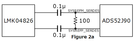


Here's a question.
1. As shown in Figure 2a, why does the waveform become dull or in-phase when the terminating resistor is placed behind the AC coupling capacitors ?
2. As in Figure 2b, is there any problem when the terminating resistor is placed before AC coupling capacitors?

Please teach me.

Best regards,
M. Tachibana

  • Hi Masanori-san,

    We recommend the AC coupling circuit shown in Figure 2b due to the internal biasing circuit for the SYSREFP_SERDES and SYSREFM_SERDES pins within the ADS52J90.
    Having the 100ohm resistor short the pins together disrupts this biasing network and leads to unpredictable behavior from the chip.
    Furthermore, the SYSREF signal can be provided single-ended using an LVCMOS clock signal on SYSREFP_SERDES while grounding the SYSREFM_SERDES pin.

    Sincerely,
    Olu
  • Hello Olu-san,

    Thank you for teaching me.
    I'll recommend the customer to place the terminating resistor in front of the AC coupling capacitors as shown in Figure 2b.

    I will ask you additional questions.

    1. In ADS52J90EVM circuits, why is the terminating resistor placed behind the AC coupling capacitors as shown in Figure 2a ?

    2. Are the terminating resistors for CLKP/CLKM and SYNC_SERDES also required to be placed in front of AC coupling capacitors?

    3. Please teach me the reason why the waveform become as shown in Figure 1a or Figure 1b. Or, please teach me the input circuit of SYNC_SERDES. Is it the same as Figure 80 in the data sheet?

    Best regards,
    M. Tachibana

  • Hi Masanori-san,

    I just re-read your post and are you saying that when you have configuration 2a, varying the frequency causes the signals to become in-phase?
    Because the signals in both pictures 1a and 1b are at the same frequency of 81.3kHz, I'm not quite sure what you meant in your original post.

    We definitely do not expect phase shifts in signals used to drive the SYSREF/SYNC pins and I am unable to recreate that behavior on the EVM. I went all the way down to 244kHz SYSREF with no phase shift but I do see the exponential clock edge due to the filter formed by coupling capacitors and bias resistors.

    Under what conditions exactly did this phase shift effect occur?

    To reduce the sensitivity of SYSREFP/SYNCP and SYSREFM/SYNCM to external noise/glitches, the termination architecture was changed to the one shown below in new board revisions.  You can see a representation of the SYNC/SYSREF internal input circuit below--it was this bias network I assumed you were using for 2a and 2b.

    CLKP and CLKM do not require the new termination as the input signal is continuous as opposed to pulsed in the case of SYSREF/SYNC.

    Sincerely,

    Olu

  • Hi Olu-san,

    Thank you for your reply.

    When the customer set the output frequency low by increasing the divider ratio of SDCLKout 3, the waveform shown in Figure 1a is appeared after turning on the power and configuring. After this, if the reference signal from CLK1in is interrupted, the waveform of Figure 1b is appeared. And once this phenomenon happens, it will not return to the waveform shown in Figure 1a unless powering it on again.

    The in-phase waveform in Figure 1b is quite unexpected. And I do not understand why this phenomenon happens even if I look at the internal circuit.
    In the latest version of ADS52J90EVM, the terminating resistor is placed in front of the AC coupling capacitor, isn't it? Is it any problem to connect 125 kΩ of pull-up resister to 3.3 V rather than connecting 50 kΩ of pull-up resister to 1.8 V?

    Best regards,
    M. Tachibana

  • Hi Masanori-san,

    When your customer captured this SYSREF signal, was the LMK04826 in bypass mode with no PLLs in operation? It's possible that the LMK04826 doesn't drive the SYSREF pins in a predictable manner when it's PLLs are not being used.

    Please check if the issue disappears when the PLLs are locked. Utilize/lock the PLLs by making the changes as described in my response to your other thread here. There is nothing in the device or EVM's termination network that should cause a phase shift.

    Also, is there a particular reason why you are disconnecting your input clock source mid-capture?

    The SYSREFP_SERDES and SYSREFM_SERDES pins are rated a max voltage of ~2.1V so using a 3.3V source to pull them up is not recommended.

    Sincerely,

    Olu

  • Hi Olu-san,

    Thank you for the information.

    Certainly the customer is currently using LMK 04826 as a bypass mode without using the PLL. And at that time the waveform becomes blunt or in phase.
    However, it is mysterious that this phenomenon is seen only at SDCLKout 3s which are connected to the ADS52J90. Under the same condition, this phenomonen doesn't appear at SDCLKout 1 connected to the external FPGA.

    Currently, the customer supplies clock to LMK 04826 from FPGA. When reconfiguring the FPGA, the clock from the FPGA is momentarily interrupted.

    I understood that SYSREFP_SERDES and SYSREFM_SERDES must be pulled up to 1.8V.

    Best regards,
    M. Tachibana

  • Hi Masanori-san,

    I actually see similar in-phase SYSREF behavior from SDCLKout1 when the LMK is in bypass mode as detailed in this post on the clocking forum.

    We'll get clarification from the clocking team on expected SYSREF behavior in bypass mode subsequently but in the mean time, I suggest you have your customer use the workaround of having locked PLLs generate the SYSREF signal from the LMK04826 to enforce deterministic latency for multiple JESD204B devices.

    Sincerely,

    Olu

  • Hi Olu-san,

    I hope that the reason why the in-phase waveform is seen in the bypass mode will be revealed.
    Please inform me if you obtain the reason.

    Best regards,
    M. Tachibana