This thread has been locked.

If you have a related question, please click the "Ask a related question" button in the top right corner. The newly created question will be automatically linked to this question.

AM335x GPMC: Speed up using EDMA and/or Burst access

Other Parts Discussed in Thread: AM3359, SYSBIOS, SYSCONFIG

Hi,

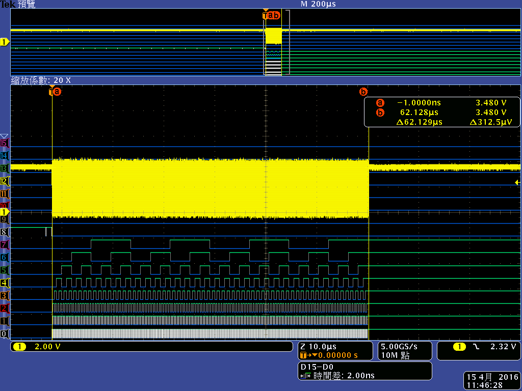
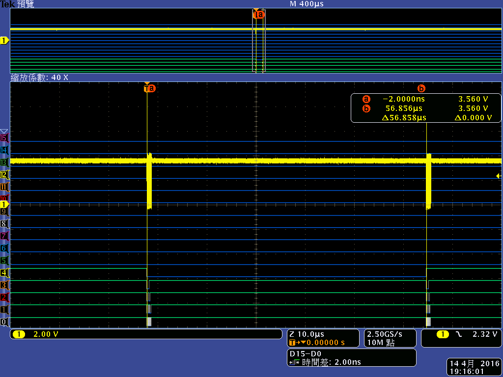
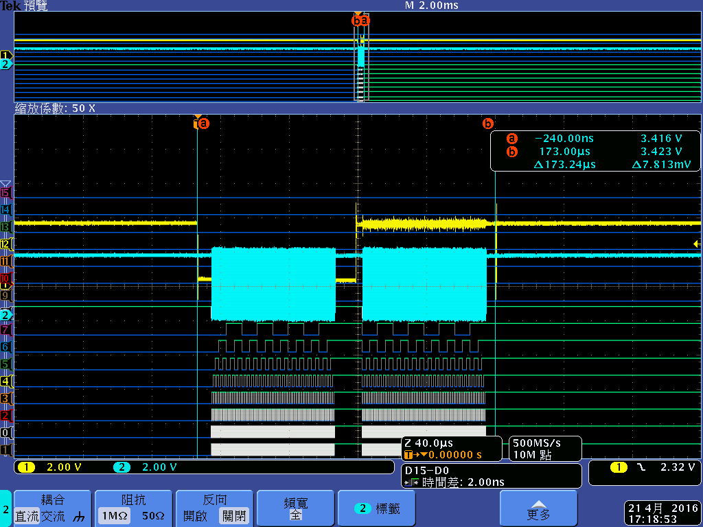
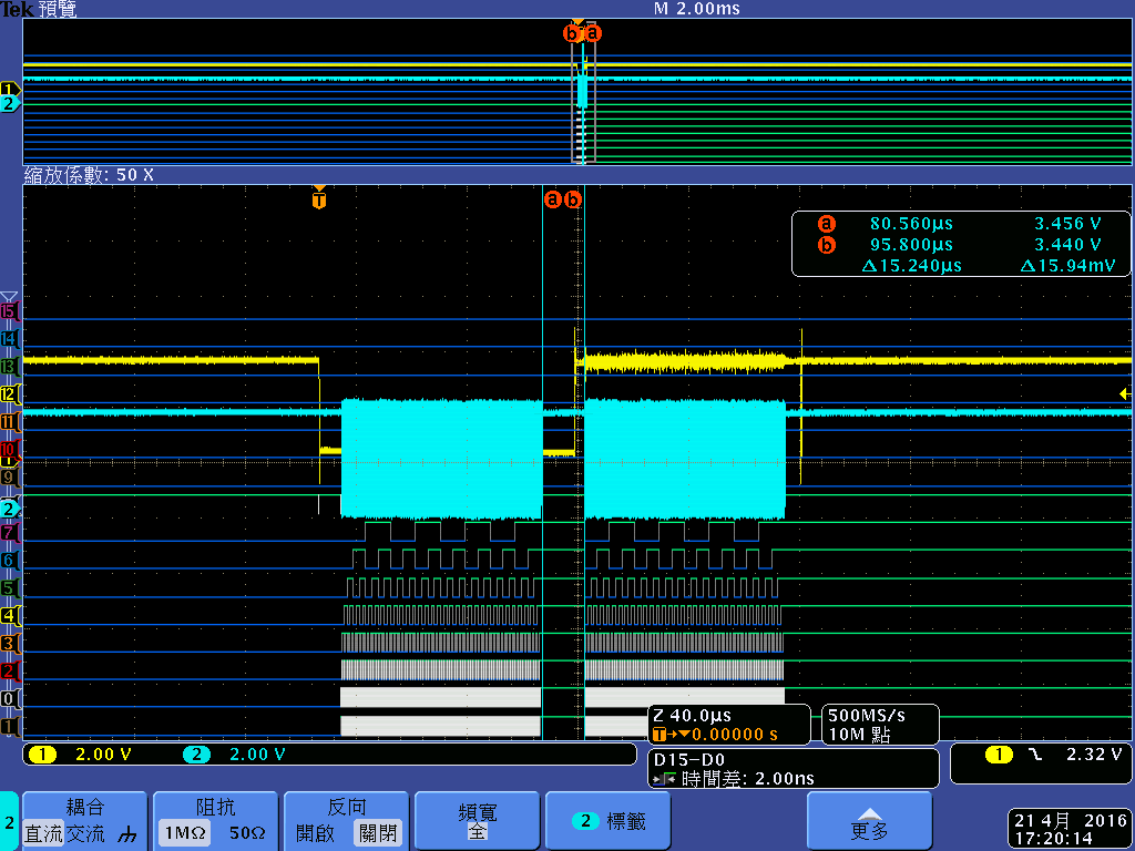
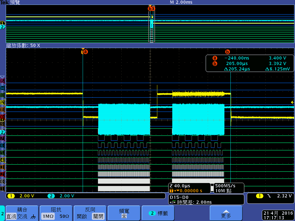
I have connected a CPLD to the AM3359 GPMC interface as an AD muxed device and found that single asynchronous read write access triggered by the CPU is much too slow for our application - we have to read/write about 32 registers within a few microseconds. This is mainly due to a 250 ns delay between the memory accesses, following Wolfgang Muees1 in

e2e.ti.com/.../331886

"the problem with the GPMC is the internal bus arbitration time. If you use single byte reads, you won't get any further."

As fas as I can see, I have the following options:

- reprogram the cpld making it understand burst accesses and/or

- use EDMA.

Following  Thomas Renjith in 

e2e.ti.com/.../216305

I have to use ASM statements to trigger burst lengths of 8 or 16 using the CPU.

My questions are:

- Will the 250 ns delay due to internal bus arbitration time vanish if I use DMA accesses in single asynchronous read/write mode?

- Can the EDMA do burst accesses if I use the right parameterization (maybe EDMA transfer controller default burst size (DBS) = GPMC ATTACHEDDEVICEPAGELENGTH ?

- My TI Code generation tools are not happy with the code examples given by Thomas Renjith for the GCC. Has anyone an example for TI CGTs? In a first quick seach into arm_assembly_language_tools_spnu118m.pdf, arm_c_compiler_spnu151j.pdf and ARM_TMS470R1xUsersGuide_spnu134b.pdf I did not find the right information how to do. The goal is to have  (assembler or better C asm inline coded) functions interfacing to C that does the burst r/w accesses. Any tips where to read about?

Thanks,

Frank

  • Hi Frank,

    fmdhr said:
    - Will the 250 ns delay due to internal bus arbitration time vanish if I use DMA accesses in single asynchronous read/write mode?

    I don't think there will be a significant improvement for single access.

    fmdhr said:
    - Can the EDMA do burst accesses if I use the right parameterization (maybe EDMA transfer controller default burst size (DBS) = GPMC ATTACHEDDEVICEPAGELENGTH ?

    Yes, this will speed up things a lot.

    fmdhr said:
    - My TI Code generation tools are not happy with the code examples given by Thomas Renjith for the GCC. Has anyone an example for TI CGTs? In a first quick seach into arm_assembly_language_tools_spnu118m.pdf, arm_c_compiler_spnu151j.pdf and ARM_TMS470R1xUsersGuide_spnu134b.pdf I did not find the right information how to do. The goal is to have  (assembler or better C asm inline coded) functions interfacing to C that does the burst r/w accesses. Any tips where to read about?

    This forum supports only Linux, can't help here.

  • Hi Biser,


    thanks for your reply. I'll try DMA first and will report what happens.

    Frank

  • Hi Biser et.al.,


    as announced here is a first report: I tried to set up EDMA access, and due to some errors in the EDMA starterware driver I changed the BIOS and XDCTools versions and ran the old code _without_ EDMA again. And - surprising news - all is much faster, the timing is as programmed (GPMC FCLK seems to be 100, not 104 MHz as stated in the TRM) - Details see below.

    Do you (or anybody else) have an explanation for that (or an idea where to find one)?

    And, bad news: my ISRs do not work any more in the CCS debug environment with the new XDCtools 3.30.5.60, BIOS 6.41.0.26. I get 2 DMTIMER interrupts, suspend and resume the program with the debugger, get 2 additional interrupts, etc.

    Would be _very_ nice to get an explanation for that, too.

    Thanks,

    Frank

    Timing measurement for access to a CPLD via GPMC, times for write cycle

    SDK 1.1.0.6, CCS  Version: 6.0.1.00040, Spectrum Digital XDS560v2 LC

    XDCtools 3.25.3.72, BIOS 6.35.4.50,
    slow timing (GPMC defaults)
    GPMC_GPMC_CONFIG1_0
    00601200
    GPMC_GPMC_CONFIG2_0
    00101001
    GPMC_GPMC_CONFIG3_0
    22060514
    GPMC_GPMC_CONFIG4_0
    10057016
    GPMC_GPMC_CONFIG5_0
    010F1111
    GPMC_GPMC_CONFIG6_0
    0F070000
    GPMC_GPMC_CONFIG7_0
    00000F41
    gives (150 + 250) ns = 400 ns (2.5 MHz) (Scope ALL 149)

    fast timing (register edit) according to Figure 7-14 SPRUH73K
    GPMC_GPMC_CONFIG1_0
    00601200
    GPMC_GPMC_CONFIG2_0
    00061001
    GPMC_GPMC_CONFIG3_0
    22030512
    GPMC_GPMC_CONFIG4_0
    05047016
    GPMC_GPMC_CONFIG5_0
    010F0711
    GPMC_GPMC_CONFIG6_0
    05040000
    GPMC_GPMC_CONFIG7_0
    00000F41
    gives (50 + 250) ns = 300 ns (3.33 MHz) (Scope ALL 150)

    WRACCESSTIME = 5, otherwise
    CortxA8: Trouble Halting Target CPU: (Error -2062 @ 0x3E418) Unable to halt device. Reset the device, and retry the operation. If error persists, confirm configuration, power-cycle the board, and/or try more reliable JTAG settings (e.g. lower TCLK). (Emulation package 5.1.641.0)

    XDCtools 3.30.5.60, BIOS 6.41.0.26
    slow timing as programmed (GPMC defaults)
    GPMC_GPMC_CONFIG1_0
    00601200
    GPMC_GPMC_CONFIG2_0
    00101001
    GPMC_GPMC_CONFIG3_0
    22060514
    GPMC_GPMC_CONFIG4_0
    10057016
    GPMC_GPMC_CONFIG5_0
    010F1111
    GPMC_GPMC_CONFIG6_0
    0F070000
    GPMC_GPMC_CONFIG7_0
    00000F41
    gives (150 + 20) ns = 170/180 ns (5.55 MHz) (Scope ALL 151)

    fast timing (register edit) according to Figure 7-14 SPRUH73K
    GPMC_GPMC_CONFIG1_0
    00601200
    GPMC_GPMC_CONFIG2_0
    00061001
    GPMC_GPMC_CONFIG3_0
    22030512
    GPMC_GPMC_CONFIG4_0
    05047016
    GPMC_GPMC_CONFIG5_0
    010F0711
    GPMC_GPMC_CONFIG6_0
    05040000
    GPMC_GPMC_CONFIG7_0
    00000F41
    gives (50 + 20) ns = 70 ns (14.3 MHz) (Scope ALL 152)
    which is the timing expected

  • fmdhr,
    Is it  Micron Nand Flash?
    Have you achieved (50+20)ns between word transfers?

    if acheived ,The gap can be further reduced by prefetch engine.

    If not acheived/further want to reduce, the areas to look into are:

    1) GPMC Config registers modifications ( as you experimented)

    2) Reduce program delay
           a) Enable instruction cache, which will improve performance drastically by caching the istructions.
           b) Reduce gaps between Istructions and 5 byte Memory transfers ( Ex: Read istruction followed by Array location to be read).
           c) Use page read cache register (It can save 20us per page read) (which will bring the time to read the Nand array to the attached Register(size 2048) .
           Note: Page read cache is availabe with Micron Nand flash. Not sure about other chips. Go through Data sheet for time taken to read the page into attached    register.
           d) Now reading from register into Memory. which can be optimized in following ways
                     i) Use ldmia and stmia istructions to read multiple instructions ( hard coding the usage of r4-r11 may not work always)
                     ii) Try to reduce the gaps between each 512 bytes read and ECC Calculations and comparision( use memcomp) and correction( Do not go for correction if comparison is good).
                    iii) Optimize the code part of Prefetch engine to read ( which will bring good performance improvement).
    Note: Configuration register modifcation may lead to problems (if all the parameters are not propotionally modifed)
    Excess Optimization may cause overlap of read cycles leading to data corruption.

    Major contributors: 1) Prefetch engine.2) Page read cache3) Instruction cache

    Regards,

    Murali Krishna Dama

  • Hi Murali Krishna Dama,

    thanks for your reply.

    Murali Dama said:
    Is it  Micron Nand Flash?

    No, it's not a Nand Flash, it's a Lattice Mach 4256 CPLD.

    Murali Dama said:
    Have you achieved (50+20)ns between word transfers?

    Yes, the AAD mode only works as 16 bit only. Although we have connected only AD[0-7] and actually read bytes only, the GPMC is programmed for word access.

    The timimg (50+20)ns is a 1st approach that meets the sequence (not times) given in Figure 7-14 of the TRM SPRUH73K and may be further optimised.

    Murali Dama said:

    2) Reduce program delay
           a) Enable instruction cache, which will improve performance drastically by caching the istructions.
           b) Reduce gaps between Istructions and 5 byte Memory transfers ( Ex: Read istruction followed by Array location to be read).
           c) Use page read cache register (It can save 20us per page read) (which will bring the time to read the Nand array to the attached Register(size 2048) .
           Note: Page read cache is availabe with Micron Nand flash. Not sure about other chips. Go through Data sheet for time taken to read the page into attached    register.
           d) Now reading from register into Memory. which can be optimized in following ways
                     i) Use ldmia and stmia istructions to read multiple instructions ( hard coding the usage of r4-r11 may not work always)
                     ii) Try to reduce the gaps between each 512 bytes read and ECC Calculations and comparision( use memcomp) and correction( Do not go for correction if comparison is good).
                    iii) Optimize the code part of Prefetch engine to read ( which will bring good performance improvement).
    Note: Configuration register modifcation may lead to problems (if all the parameters are not propotionally modifed)
    Excess Optimization may cause overlap of read cycles leading to data corruption.

    Major contributors: 1) Prefetch engine.2) Page read cache3) Instruction cache

    Instruction cache is enabled, code runs from cached DDR3. Your other information is for Nands only as far as I can see and does not match our case.

    The code the timing was measured with is

                /* write at address i the data ~i to get A/D toggle on the scope */
                for ( i = 0; i < 256; ++i ) {
                    cpld_register.cpld_register16[i] = ~i;
                }
       
    (As you can see, there are some more ops as the memory access only.) The use of special assembler instructions ldmia, stmia would require information about interfacing this with C, as I asked in my former posting.

    What I really wanted to know: Why does it work with the newer BIOS / XDC and not with the older one?

    To get an answer to my second important question (blocked ISRs), I opened a new thread: e2e.ti.com/.../411365

    Thanks

    Frank

  • Sorry, there was a typo: Of course t is AD muxed mode only, not AAD muxed mode.

    Frank
  • Still waiting for an answer...

    Frank
  • Hello All,

                  That's great fmdhr, u achieved the required throughput to access the CPLD. Our scenario is almost same except instead of CPLD, We are using FPGA (Address & Data non - multiplexed bus & Synchronous). We are using Starterware GPMC Driver to acccess the FPGA & TI Compiler 5.1.9. We are also facing the same problems mentioned above.The throughput is less as compared to the Actual theoretical results. Please guide us to sort out the problem, in the starter ware.

    I would like to know, is there any dependencies in the compiler for GPMC bus arbitration time ?

    Is it required to port the Starter ware project to SYS/BIOS Project?       

    Thanks & Regards

    Rama Krishna

  • Hi,

    rama krishna said:
    I would like to know, is there any dependencies in the compiler for GPMC bus arbitration time ?

    I think it is rather a problem with MMU/Cache configuration. As you might have noticed, I had a problem with ISRs too. I discussed it with Scott Gary from TI in the thread:

    I found out that ISRs are working with a different MMU initialisation (but cannot explain why). And, concerning GPMC timing, I have

    Bad News:

    With the new MMU initialisation that makes ISRs working, the GPMC timing is AS SLOW AS BEFORE. So the code from C:\ti\am335x_sysbios_ind_sdk_1.1.0.6\sdk\os_drivers\src\osdrv_mmu.c should be read as

    #if YOU_WANT_WORKING_ISRs_AND_SLOW_GPMC_TIMING

    #if (ti_sysbios_family_arm_a8_Mmu___VERS >= 160)
            if (!attrs.bufferable && !attrs.cacheable)
                attrs.tex = 0; //tex is initialized to 1 and need this to force strongly ordered
    #endif

    #else

    /* YOU_GET_FAST_GPMC_TIMING_BUT_NO_WORKING_ISRs */

    #endif

    Means, that you have the choice between Scylla and Charybdis.

    Worst case may be, that the fast timing I measured is working only accidentially - and there are other things going wrong deep inside the ARM architecture, and we finally must use EDMA and/or burst access...

    In my SYS/BIOS environment, the code for MMU/Cache comes from C:\ti\bios_6_41_00_26\packages\ti\sysbios\family\arm\a8\*. I don't know exactly how this is done with starterware / linux (I have seen some code for cache initialisation in the starterware too).

    As far as I can see, the MMU/Cache is controlled by the CP15 coprocessor, and AM335x_technical_reference_manual_spruh73k.pdf won't help you, see e.g. the ARM documentation DDI0406C_C_arm_architecture_reference_manual.pdf instead.

    Hope that Scott Gary and the TI team find an answer...

    Regards,

    Frank

  • Hi,

    Can you try setting GPM config register to Device type i.e. add below configuration to SYS_MMU_ENTRY applMmuEntries[]

       {(void*)0x50000000, SYS_MMU_BUFFERABLE },

  • Hello fmdhr,

                     Please look into the My MMU Configuration, i have not go through in detail about the MMU of AM335x.After seeing your post , i recheck the MMU Configuration, noticed that the device memory marked as normal memory and some cache attributes.


    void MMUConfigAndEnable(void) {

    /*DDR Configuration*/

        REGION regionDdr = { MMU_PGTYPE_SECTION, START_ADDR_DDR, NUM_SECTIONS_DDR,
                MMU_MEMTYPE_NORMAL_NON_SHAREABLE(MMU_CACHE_WT_NOWA,
                        MMU_CACHE_WB_WA), MMU_REGION_NON_SECURE,
                MMU_AP_PRV_RW_USR_RW, (unsigned int*) pageTable };

        /*
         ** Define OCMC RAM region of AM335x. Same Attributes of DDR region given.
         */

        REGION regionOcmc = { MMU_PGTYPE_SECTION, START_ADDR_OCMC,
                NUM_SECTIONS_OCMC,
                MMU_MEMTYPE_NORMAL_NON_SHAREABLE(MMU_CACHE_WT_NOWA,
                        MMU_CACHE_WB_WA), MMU_REGION_NON_SECURE,
                MMU_AP_PRV_RW_USR_RW, (unsigned int*) pageTable };

        /*
         ** Define SRAM region of AM335x. Same Attributes of DDR region given.
         */
      

     REGION regionSram = { MMU_PGTYPE_SECTION, START_ADDR_SRAM,
                NUM_SECTIONS_SRAM,
                MMU_MEMTYPE_NORMAL_NON_SHAREABLE(MMU_CACHE_WT_NOWA,
                        MMU_CACHE_WB_WA), MMU_REGION_NON_SECURE,
                MMU_AP_PRV_RW_USR_RW, (unsigned int*) pageTable };

        /*
         ** Define Device Memory Region. The region between OCMC and DDR is
         ** configured as device memory, with R/W access in user/privileged modes.
         ** Also, the region is marked 'Execute Never'.
         */
        REGION regionDev = { MMU_PGTYPE_SECTION, START_ADDR_DEV, NUM_SECTIONS_DEV,
                MMU_MEMTYPE_DEVICE_SHAREABLE, MMU_REGION_NON_SECURE,
                MMU_AP_PRV_RW_USR_RW | MMU_SECTION_EXEC_NEVER,
                (unsigned int*) pageTable };

        REGION regionDev1 = { MMU_PGTYPE_SECTION, 0x02000000, 16,
                MMU_MEMTYPE_NORMAL_NON_SHAREABLE(MMU_CACHE_WT_NOWA,
                        MMU_CACHE_WB_NOWA), MMU_REGION_NON_SECURE,
                MMU_AP_PRV_RW_USR_RW | MMU_SECTION_EXEC_NEVER,
                (unsigned int*) pageTable };

        /* Initialize the page table and MMU */
        MMUInit((unsigned int*) pageTable);

        /* Map the defined regions */
        MMUMemRegionMap(&regionDdr);
        MMUMemRegionMap(&regionOcmc);
        MMUMemRegionMap(&regionSram);
        MMUMemRegionMap(&regionDev);
        MMUMemRegionMap(&regionDev1);
        /* Now Safe to enable MMU */
        MMUEnable((unsigned int*) pageTable);
    }

    What is the difference between sharable and non sharable memory?

    Please share your MMU Configuration for higher GPMC Speed?

    Thanks & Regards

    Rama Krishna

  • Pratheesh,

    I had the idea to use different MMU settings for memory mapped registers (e.g. 0x50000000 for GPMC) and the CPLD / FPGA memory area (0x01000000 in my implementation) that morning too (both regions were set to 0 until now). As far as I remember, MMU enrties were set to 0 (not cacheable / bufferable) for the registers in the SDK examples. It is possible that the CPLD memory region should be set to "Device type" (what does that mean?), i.e. {(void*)0x01000000, SYS_MMU_BUFFERABLE } to get fast GPMC access?

    As already mentioned, the BIOS API reference manual is not very enlightening here.

    I cannot find out it today, because I'm not at the office, its holyday in Germany.

    Thanks

    Frank

  • Frank,

    infocenter.arm.com/.../index.jsp

    The Device memory attribute is defined for memory locations where an access to the location can cause side effects, or where the value returned for a load can vary depending on the number of loads performed. Memory-mapped peripherals and I/O locations are typical examples of areas of memory that you must mark as Device

    We have seen up to 4X improvements by setting BUFFERABLE for register accesses (specially write operations). SDK examples are not completely optimized. We are planning to make this change in future releases.
  • Hi Pratheesh,


    sorry for the late response. Unfortunable, the thread has been split into two threads, I don't know why...

    Your link to the arm infocenter points to an ARM 11 documentation, an ARMv6 implementation, but AM335x is a v7 implementation, so I think ARM® Architecture Reference Manual ARMv7-A and ARMv7-R edition ARM DDI 0406C.c is more accurate.

    The mmu init function in \am335x_sysbios_ind_sdk_1.1.0.6\sdk\os_drivers\src\osdrv_mmu.c is not able to set device type memory (TEX C B = 000 0 1) and should be updated in future releases. I had to use BIOS function Mmu_setFirstLevelDesc (see below) to set shareable device type memory. And of course you have to set this for the device (0x0100 0000), not for the GPMC configuration registers (0x5000 0000).

    Using this, I got fast cpu writes (no additional 250 ns delay), but not so fast cpu reads (with 250 ns delay after each 16, 32, 64 bit access), details see below.

    Finally, I meanwhile set up my EDMA. With this, I get both fast reads and writes in asynch. single r/w accesses - exactly the programmed GPMC_CONFIG5_0_RDCYCLETIME and GPMC_CONFIG5_0_WRCYCLETIME, no intermediate delays.

    [Quote of Biser Gatchev, Mar 20th:]

    Hi Frank,

    fmdhr
    - Will the 250 ns delay due to internal bus arbitration time vanish if I use DMA accesses in single asynchronous read/write mode?

    I don't think there will be a significant improvement for single access.

    [End Quote]

    I think, there is an improvement.

    Regards,

    Frank

        /*
        assumes TRE (TEX remap enabled) = 0 and AFE (access flag enable) = 0
        in the CP15_CONTROL_REGISTER (SCTLR)
        TEX[2:0] and C, B  determine memory type:
        shareable device memory is 000 0 1
        */
        /* set default attributes */
        Mmu_initDescAttrs(&attrs);
        /* change attributes for cpld */
        attrs.type = Mmu_FirstLevelDesc_SECTION;
        attrs.cacheable = 0;
        attrs.bufferable = 1;
        attrs.tex = 0;
        attrs.domain = 0;
        attrs.imp = 1;      // implementation specific
        attrs.accPerm = 3;  // access permission: read/write
        attrs.shareable = 0;

        /* program mmu for cpld access (MMUIinit cannot set this combination) */
        Mmu_disable();
        Mmu_setFirstLevelDesc((Ptr)&cpld_register, (Ptr)&cpld_register, &attrs);
        Mmu_enable();

    ARM® Architecture Reference Manual ARMv7-A and ARMv7-R edition ARM DDI 0406C.c

    Table B3-10 TEX, C, and B encodings when TRE == 0, p. B3-1367, my measurements supplemented:

    CPU access results (TRE = AFE = 0 in control register: CP15_CONTROL_REGISTER (SCTLR))

    TEX C B  Description        Memory type         Shareable   desc    w16     r16     w32     r32     w64     r64    
    -----------------------------------------------------------------------------------------------------------------
    000 0 0 Strongly-ordered    Strongly-ordered    Shareable   0e02    s       s       fs      fs(0)   fffs    fffs    
    000 0 1 Shareable Device    Device              Shareable   0e06    f       s       f       fs      ffff    fffs    
    000 1 0 O & I WT nWA        Normal              S bitb      -       -
    000 1 1 O & I WB nWA        Normal              S bitb      0e0e    f(1)
    001 0 0 O & I Non-cacheable Normal              S bitb      1e02    f(1)
    001 0 1 Reserved            -                   -           1e06    f(1)    s
    001 1 0 impl. defd.         impl. defd.         impl.d.     1e0a    f(1)
    001 1 1 O & I WB WA         Normal              S bitb      1e0e    f(2)  
    010 0 0 Non-shareable Dev.  Device              Non-shrbl   1e02    (3)
    010 0 1 Reserved            -                   -           -       -
    010 1 x Reserved            -                               -       -
    011 x x Reserved            -                               -       -
    1BB A A Cacheable memory    Normal              S bitb      -       -
    AA = Inner attributec
    BB = Outer attribute

    Explanations:

    desc = lower bits of short-descriptor memory region attributes (0x1000 4 byte entries for all the 1 MB regions)
    wXX, rXX = cpu access to XX = 16, 32, 64 bit values (uint16_t, uint32_t, uint64_t)

    f = fast access in programmed cycle time
    s = slow access with additional 250 ns delay

    (0) additional time in 1st access
    (1) no 2nd access (error!)
    (2) write does a read (error!)
    (3) system crash

  • Hello Rama Krishna,

    I don't know how to set up the MMU using the starterware functions. Finally, both all the BIOS and Starterware programming should result in the same 'First Level Descriptor Table' entries used by the ARM CP15 hardware. Details see my other positing.

    Hope this helps a bit.

    Frank
  • Hi Frank:

    I use CCS V6,am335x_sysbios_ind_sdk_1.1.0.8,bios_6_41_04_54,ndk_2_24_01_18 and xdctools_3_30_06_67_core.


    I follow your suggestion likes below but it has no help, it still with additional 250 ns delay.

    /* set default attributes */
    Mmu_initDescAttrs(&attrs);
    /* change attributes for cpld */
    attrs.type = Mmu_FirstLevelDesc_SECTION;
    attrs.cacheable = 0;
    attrs.bufferable = 1;
    attrs.tex = 0;
    attrs.domain = 0;
    attrs.imp = 1; // implementation specific
    attrs.accPerm = 3; // access permission: read/write
    attrs.shareable = 0;

    /* program mmu for cpld access (MMUIinit cannot set this combination) */
    Mmu_disable();
    Mmu_setFirstLevelDesc(0x100000, (Ptr)&cpld_register, &attrs);
    Mmu_enable();

    Maybe I misunderstand what you mean,please correct me, if I am wrong.

    And I also try edma_Test in starterware directory to test EDMA transfer.

    However, it does not work.

    Does EDMA must use GPMC burst setting?

    Could you give me some suggestion?

    Best regards,

    Marcus
  • lu yuenjune said:
    Hi Frank:

    I use CCS V6,am335x_sysbios_ind_sdk_1.1.0.8,bios_6_41_04_54,ndk_2_24_01_18 and xdctools_3_30_06_67_core.


    I follow your suggestion likes below but it has no help, it still with additional 250 ns delay.

    /* set default attributes */
    Mmu_initDescAttrs(&attrs);
    /* change attributes for cpld */
    attrs.type = Mmu_FirstLevelDesc_SECTION;
    attrs.cacheable = 0;
    attrs.bufferable = 1;
    attrs.tex = 0;
    attrs.domain = 0;
    attrs.imp = 1; // implementation specific
    attrs.accPerm = 3; // access permission: read/write
    attrs.shareable = 0;

    /* program mmu for cpld access (MMUIinit cannot set this combination) */
    Mmu_disable();
    Mmu_setFirstLevelDesc(0x100000, (Ptr)&cpld_register, &attrs);
    Mmu_enable();

    Maybe I misunderstand what you mean,please correct me, if I am wrong.

    And I also try edma_Test in starterware directory to test EDMA transfer.

    However, it does not work.

    Does EDMA must use GPMC burst setting?

    Could you give me some suggestion?

    Best regards,

    Marcus

    Hi Marcus,


    sorry for the late response (I wasn't in the office last week). And sorry, it's a long time ago I dealt with the problem.

    If your external memory is controlled by the GPMC, I assume you have prorammed the GPMC registers GPMC_CONFIG[1-7](CS_AREA) correctly. E.g.:

        GPMCClkConfig();

        /* pin multiplexing is already done via central table */

        /* gpmc reset */
        /* GPMCModuleSoftReset(unsigned int baseAddr) */
        HWREG(baseAddr + GPMC_SYSCONFIG) = (GPMC_SYSCONFIG_SOFTRESET_RESET <<
                                           GPMC_SYSCONFIG_SOFTRESET_SHIFT);
        /* wait until reset is done */
        /* GPMCModuleResetStatusGet(unsigned int baseAddr) */
        while ( !(HWREG(baseAddr + GPMC_SYSSTATUS) & GPMC_SYSSTATUS_RESETDONE) );

        /* configure wait pin (optional) */
        // HWREG(baseAddr + GPMC_SYSCONFIG) =

        /* program GPMC_CONFIG1, see 7.1.6.11 GPMC_CONFIG1_0 Register */
        /* configure for asynchronous single read and write access with ad mux */

        HWREG(baseAddr + GPMC_CONFIG1(CPLD_CS)) =
          /* bit fields in alphabetical order as in hw_gpmc.h */
          ((GPMC_CONFIG1_0_ATTACHEDDEVICEPAGELENGTH_FOUR << GPMC_CONFIG1_0_ATTACHEDDEVICEPAGELENGTH_SHIFT) &
              GPMC_CONFIG1_0_ATTACHEDDEVICEPAGELENGTH) |
          ((GPMC_CONFIG1_0_CLKACTIVATIONTIME_ATSTART << GPMC_CONFIG1_0_CLKACTIVATIONTIME_SHIFT) &
              GPMC_CONFIG1_0_CLKACTIVATIONTIME)|
          ((GPMC_CONFIG1_0_DEVICESIZE_SIXTEENBITS << GPMC_CONFIG1_0_DEVICESIZE_SHIFT) &
                  GPMC_CONFIG1_0_DEVICESIZE) |
          ((GPMC_CONFIG1_0_DEVICETYPE_NORLIKE << GPMC_CONFIG1_0_DEVICETYPE_SHIFT) &
                  GPMC_CONFIG1_0_DEVICETYPE) |
          ((GPMC_CONFIG1_0_GPMCFCLKDIVIDER_DIVBY1 << GPMC_CONFIG1_0_GPMCFCLKDIVIDER_SHIFT) &
                  GPMC_CONFIG1_0_GPMCFCLKDIVIDER) |
          ((GPMC_CONFIG1_0_MUXADDDATA_MUX << GPMC_CONFIG1_0_MUXADDDATA_SHIFT) &
                  GPMC_CONFIG1_0_MUXADDDATA) |
          ((GPMC_CONFIG1_0_READMULTIPLE_RDSINGLE << GPMC_CONFIG1_0_READMULTIPLE_SHIFT) &
                  GPMC_CONFIG1_0_READMULTIPLE) |
          ((GPMC_CONFIG1_0_READTYPE_RDASYNC << GPMC_CONFIG1_0_READTYPE_SHIFT) &
                  GPMC_CONFIG1_0_READTYPE) |
          ((GPMC_CONFIG1_0_TIMEPARAGRANULARITY_X1 << GPMC_CONFIG1_0_TIMEPARAGRANULARITY_SHIFT) &
                  GPMC_CONFIG1_0_TIMEPARAGRANULARITY) |
          ((GPMC_CONFIG1_0_WAITMONITORINGTIME_ATVALID << GPMC_CONFIG1_0_WAITMONITORINGTIME_SHIFT) &
                  GPMC_CONFIG1_0_WAITMONITORINGTIME) |
          ((GPMC_CONFIG1_0_WAITPINSELECT_W0 << GPMC_CONFIG1_0_WAITPINSELECT_SHIFT) &
                  GPMC_CONFIG1_0_WAITPINSELECT) |
          /* no wait monitoring for read */
          ((GPMC_CONFIG1_0_WAITREADMONITORING_WNOTMONIT << GPMC_CONFIG1_0_WAITREADMONITORING_SHIFT)
              & GPMC_CONFIG1_0_WAITREADMONITORING) |
          /* no wait monitoring for write */
          ((GPMC_CONFIG1_0_WAITWRITEMONITORING_WNOTMONIT << GPMC_CONFIG1_0_WAITWRITEMONITORING_SHIFT)
              & GPMC_CONFIG1_0_WAITWRITEMONITORING) |
          ((GPMC_CONFIG1_0_WRAPBURST_WRAPNOTSUPP << GPMC_CONFIG1_0_WRAPBURST_SHIFT) &
                  GPMC_CONFIG1_0_WRAPBURST) |
          ((GPMC_CONFIG1_0_WRITEMULTIPLE_WRSINGLE << GPMC_CONFIG1_0_WRITEMULTIPLE_SHIFT) &
                  GPMC_CONFIG1_0_WRITEMULTIPLE) |
          ((GPMC_CONFIG1_0_WRITETYPE_WRASYNC << GPMC_CONFIG1_0_WRITETYPE_SHIFT) &
                  GPMC_CONFIG1_0_WRITETYPE);

    And so on. This sets the primary timings, and you can check this using CPU accesses and a Scope. (Maybe there are delays, you may check byte, word, dword accesses).

    EDMA: I cannot remember if I got the example running. Generally, I'm not very happy with the Starterware examples.

    Here the essentials of my EDMA setup (using some starterware functions from C:\ti\am335x_sysbios_ind_sdk_1.1.0.8\sdk\starterware\drivers\edma.c) (Triggered by external pin):

        /* configure EDMA module clock */
        EDMAModuleClkConfig();

        /* initialize EDMA event channel */
        EDMA3Init(SOC_EDMA30CC_0_REGS, CPLD_DMA_EVTQ);

        /* request DMA channel and TCC */
        /*
        does a lot of strange things, TCC is overwritten in SetPaRAM ...,
        Interrupt is enabled
        */
        retVal = EDMA3RequestChannel(SOC_EDMA30CC_0_REGS,
                                     CPLD_DMA_CH_TYPE, CPLD_DMA_READ_CH_NUM,
                                     CPLD_DMA_READ_TCC, CPLD_DMA_EVTQ);
        /* TODO: check retval */

        /* necessary ? */
        EDMA3EnableChInShadowReg(SOC_EDMA30CC_0_REGS, EDMA3_CHANNEL_TYPE_DMA,
                                    CPLD_DMA_READ_CH_NUM);

        /* prepare edma parameter sets - use configured parameters (copy) */

         /* write the linked PaRAM sets */
        edma_read_params.destAddr = (unsigned int)&scn_cpld_regs_readbuf[1][0];
        EDMA3SetPaRAM(SOC_EDMA30CC_0_REGS, CPLD_DMA_READ_LK_NUM,
                      &edma_read_params);
     
        /* write the PaRAM sets directly used by the channels */
        edma_read_params.destAddr = (unsigned int)&scn_cpld_regs_readbuf[0][0];
        EDMA3SetPaRAM(SOC_EDMA30CC_0_REGS, CPLD_DMA_READ_CH_NUM,
                      &edma_read_params);
     
     
        /*
        before we start the edma, the data buffers it reads from must be
        initialised, this is done by the cpld_set_* function in cpld_start()
        */

        /*
        give EDMATC0 a higher priority than mmu, pru_icss, etc. to ensure transfer
        in hard real time (10 us)
        see TRM 9.2.4.3.1 Initiator Priority Control for Interconnect
        0 = low, 1 = medium, 3 = high priority, initally all priorities are = 0
        */
        HWREG(SOC_CONTROL_REGS + CONTROL_INIT_PRIORITY(0)) |=
          ((1 << CONTROL_INIT_PRIORITY_0_TCRD0_SHIFT) & CONTROL_INIT_PRIORITY_0_TCRD0) |
          ((1 << CONTROL_INIT_PRIORITY_0_TCWR0_SHIFT) & CONTROL_INIT_PRIORITY_0_TCWR0);

        /* prepare interrupts */
        // EDMA3EnableEvtIntr(SOC_EDMA30CC_0_REGS, CPLD_DMA_EACK_CH_NUM)
        /* interrupt enable set register (IESR) */
        HWREG(SOC_EDMA30CC_0_REGS + EDMA3CC_S_IESR(0)) |=
            (1 << CPLD_DMA_EACK_CH_NUM);

        /************ set up GPIO to generate start event(s) for EDMA *************/

        /* set up gpio event detection: choose rising edge as event source */
        HWREG(CPLD_EVTPIN_GPIO_BASEADDRESS + GPIO_RISINGDETECT) |=
                1 << CPLD_EVTPIN_GPIO_PINNUMBER;
        /* IRQ 0 must be activated too to enable dma event generation */
        HWREG(CPLD_EVTPIN_GPIO_BASEADDRESS + GPIO_IRQSTATUS_SET(0)) |=
                1 << CPLD_EVTPIN_GPIO_PINNUMBER;
        /* enable DMA event generation by writing 0 to DMAEvent_Ack field in EOI */
        HWREG(CPLD_EVTPIN_GPIO_BASEADDRESS + GPIO_EOI) = 0;

        /* enable the external event for the used channel */
        HWREG(SOC_EDMA30CC_0_REGS + EDMA3CC_EESR) |= (1 << CPLD_DMA_READ_CH_NUM);

    // pin mux and GPIOs must be set too....

    ...

    void
    hwiFxn_cpld_edmatc()
    {
        uint32_t    ipr;    /* edma interrupt pending register */

        /* handle interrupts 0 to 31 only */
        ipr = HWREG(SOC_EDMA30CC_0_REGS + EDMA3CC_S_IPR(0));
        /* reset interrupt flag in edma registers */
        HWREG(SOC_EDMA30CC_0_REGS + EDMA3CC_S_ICR(0)) = ipr;

        // make sure the event comes again...(reset GPIO flag etc.)

    }

    A pitfall is the selection of channel and event, here my notes: 

    see AM335x TRM SPRUH73K chapter 11.3.20 EDMA Events
    see AM335x TRM SPRUH73M chapter 11.3.19 EDMA Events p. 1544
    EDMA Events (Event == Channel) Table 11-23. Direct Mapped:
    19 SPIREVT1 McSPI0
    20 Open Open
    21 Open Open
    22 GPIOEVT0 GPIO0
    23 GPIOEVT1 GPIO1

    see AM335x TRM SPRUH73K chapter 9.2.3 EDMA Event Multiplexing:
    use direct channel mapping, tpcc_evt_mux_20_23 in control module not programmed
    (reset value = 0)

    The PaRAM sets must be set very carefully too...

    BTW, EDMA description in revision M of the TRM is still wrong (There are 4 shadow units only in the AM3359.)

    Hope this helps

    Frank

  • Hi Frank :

    I appreciate your detail explanation about GPMC and EDMA.

    Do you shorten GPMC 250 ns bus arbitration by using burst mode or EDMA?

    In my platform, GPMC connects FPGA using non-multiplex and 16 bits mode.

    I can access FPGA using Synchronous single Access mode and I want to shorten 250 ns bus arbitration.

    Below is my GPMC configuration.

    #define BSP_GPMC_CONFIG1 0x28001000 

    #define BSP_GPMC_CONFIG2 0x00050500 

    #define BSP_GPMC_CONFIG3 0x00020202 

    #define BSP_GPMC_CONFIG4 0x05000500 

    #define BSP_GPMC_CONFIG5 0x02050505 

    #define BSP_GPMC_CONFIG6 0x50000000

    I try use EDMA to shorten bus arbitration and I use source code below for receive.

    static unsigned int GPMCNANDRxDmaConfig(unsigned int csBaseAddr, unsigned char *data,unsigned int len)
    {
    EDMA3CCPaRAMEntry paramSet;
    /* Fill the PaRAM Set with transfer specific information */
    paramSet.aCnt = GPMC_NAND_PREFETCH_FIFO_THRLD;
    paramSet.bCnt = (len/GPMC_NAND_PREFETCH_FIFO_THRLD);
    paramSet.bCntReload = 0u;
    paramSet.cCnt = 1u;
    paramSet.destAddr = (unsigned int )(data);
    paramSet.destBIdx = GPMC_NAND_PREFETCH_FIFO_THRLD;
    paramSet.destCIdx = 1;
    paramSet.linkAddr = 0xFFFFu;
    paramSet.srcAddr = csBaseAddr;
    paramSet.srcBIdx = 0;
    paramSet.srcCIdx = 0;
    paramSet.opt = 0x00000000u;
    /* Src & Dest are in INCR modes */
    paramSet.opt &= 0xFFFFFFFCu;
    /* Setting the Transfer Complete Code(TCC). */
    paramSet.opt |= (( GPMC_EDMA_TCC_NUM << EDMA3CC_OPT_TCC_SHIFT)
    & EDMA3CC_OPT_TCC);
    /* Enabling the Completion Interrupt. */
    paramSet.opt |= (1 << EDMA3CC_OPT_TCINTEN_SHIFT);
    /* Now, write the PaRAM Set. */
    EDMA3SetPaRAM(SOC_EDMA30CC_0_REGS, GPMC_EDMA_CHANNEL_NUM, &paramSet);
    /* Now enable the transfer */
    return EDMA3EnableTransfer(SOC_EDMA30CC_0_REGS, GPMC_EDMA_CHANNEL_NUM,
    EDMA3_TRIG_MODE_EVENT);
    }

    My question is since I use the 16-bit mode for FPGA, is there something wrong with code above?

    Because the code above refer nandReadWrite.c which is in starterware directory and it uses 8-bit mode for flash.

    Another question is that does EDMA must use page/burst mode for GPMC configuration?


    Please give me some suggestions.

    Sorry for bothering you again.

    Best regards,

    Marcus

  • Hi Marcus,

    I see you have choosen GPMC_CONFIG1_0_DEVICETYPE_NORLIKE in your GPMC configuration, which is IMHO the correct setting for all the things like CPLDs, FPGAs, SRAMs etc. I assume your other GPMC settings meet the needs of your FPGA memory interface, so that you get correct (maybe slow) read/write accesses.

    NAND burst access (the GPMC can do too) is "something completely different" and is not related to the 250 ns delay problem here, I think. The delay comes from the bus arbitration (L3, L4 ?) inside the AM335x.

    If you have a 16 bit interface, you may try something like this (in a loop or so):

    int16_t i1, i2; int32_t l1;

    int16_t *ptr2fpga = FPGA_ADDRESS;

    /* two accesses with 250 ns delay (?) */

    i1 = *((int16_t *)ptr2fpga);

    i2 = *(((int16_t *)ptr2fpga) + 1);

    /* 32 bit access results in 2 x 16 bit access without delay between (?) */

    l1 = *((int32_t *)ptr2fpga);

    Of course, paramSet.aCnt = GPMC_NAND_PREFETCH_FIFO_THRLD also affects the access (I think this is big enough). I use ACNT = 1 (see below).

    See also AM335x Technical Reference Manual: 11.3.12 EDMA3 Transfer Controller (EDMA3TC) and 11.3.14 EDMA3 Prioritization.

    Below some more of my settings.

    Just another tip: Cache settings may be an issue too, I use Cache_inv, Cache_wb, Cache_wait calls to synchronise CPU accesses to the AM335x memory areas read / written by the EDMA.

    Regards

    Frank

    Here my GPMC settings that result in 70 ns / 80 ns read / write cycles using EDMA (times are choosen conservatively, fast enough for us):

    GPMC_CONFIG1_0    0x00001200    The configuration 1 register sets signal control parameters per chip select. [Memory Mapped]    
    GPMC_CONFIG2_0    0x00070600    Chip-select signal timing parameter configuration. [Memory Mapped]    
    GPMC_CONFIG3_0    0x22030210    ADV# signal timing parameter configuration. [Memory Mapped]    
    GPMC_CONFIG4_0    0x06056512    WE# and OE# signals timing parameter configuration. [Memory Mapped]    
    GPMC_CONFIG5_0    0x01040807    RdAccessTime and CycleTime timing parameters configuration. [Memory Mapped]    
    GPMC_CONFIG6_0    0x05040000    WrAccessTime, WrDataOnADmuxBus, Cycle2Cycle, and BusTurnAround parameters configuration [Memory Mapped]    
    GPMC_CONFIG7_0    0x00000F41    Chip-select address mapping configuration. [Memory Mapped]    


    static EDMA3CCPaRAMEntry edma_read_params =
    {
        /* OPT - transfer options */
        /* PRIV and PRIVID are RO */
        /* Intermediate and final transfer complete chaining sets bit in CER if enabled. */
        /* Intermediate transfer complete chaining disabled (0) / enabled (1) */
        ((1 << EDMA3CC_OPT_ITCCHEN_SHIFT) & EDMA3CC_OPT_ITCCHEN) |
        /* Transfer complete chaining disabled (0) / enabled (1) */
        ((1 << EDMA3CC_OPT_TCCHEN_SHIFT) & EDMA3CC_OPT_TCCHEN) |
        /* Intermediate transfer complete interrupt is disabled (0) / enabled (1). */
        ((0 << EDMA3CC_OPT_ITCINTEN_SHIFT) & EDMA3CC_OPT_ITCINTEN) |
        /* Transfer complete interrupt is disabled (0) / enabled (1). */
        ((0 << EDMA3CC_OPT_TCINTEN_SHIFT) & EDMA3CC_OPT_TCINTEN) |
        /* Transfer complete code. This 6-bit code sets the  bit in (CER [TCC]) */
        ((CPLD_DMA_READ_TCC << EDMA3CC_OPT_TCC_SHIFT) & EDMA3CC_OPT_TCC) |
        /* Xfer completed after data xferred (NORMAL) or Xfer initiated (EARLY) */
        ((EDMA3CC_OPT_TCCMOD_EARLY << EDMA3CC_OPT_TCCMOD_SHIFT) & EDMA3CC_OPT_TCCMOD) |
        /* FIFO Width 8, 16, 32, 64, 128 or 256 bit */
        ((EDMA3CC_OPT_FWID_256BIT << EDMA3CC_OPT_FWID_SHIFT) & EDMA3CC_OPT_FWID) |
        /* 1 = static. The PaRAM set is not updated after TR */
        ((0 << EDMA3CC_OPT_STATIC_SHIFT) & EDMA3CC_OPT_STATIC) |
        /* SYNCDIM: event triggers ACNT (0 = A) or ACNT * BCNT bytes (1 = AB) */
        ((1 << EDMA3CC_OPT_SYNCDIM_SHIFT) & EDMA3CC_OPT_SYNCDIM) |
        /* destination address mode: 0 = increment, 1 = constant */
        ((0 << EDMA3CC_OPT_DAM_SHIFT) & EDMA3CC_OPT_DAM) |
        /* source address mode: 0 = increment, 1 = constant */
        ((0 << EDMA3CC_OPT_SAM_SHIFT) & EDMA3CC_OPT_SAM),
        /* SRC - byte address of source */
        (unsigned int)&cpld_register.stsx0,
        /* ACNT - count 1st dimension */
        1,
        /* BCNT - count 2nd dimension */
        sizeof(struct scn_cpld_regs_cin),
        /* DST - byte address destination */
        (unsigned int)&scn_cpld_regs_readbuf,
        /* SRCBIDX - source BCNT index: read from every 2nd byte */
        2,
        /* DSTBIDX - destination BCNT index */
        1,
        /* LINK - param address (byte offset in PaRAM), 0xffff = null link */
        EDMA3CC_OPT(CPLD_DMA_READ_LK_NUM),
        /* BCNT reload - not used in AB synced transfers */
        0,
        /* SRCCIDX - source CCNT index */
        0, /* always read the same cpld registers */
        /* DSTCIDX - destination CCNT index */
        sizeof(struct scn_cpld_regs_cin),
        /* CCNT */
        SCNCPLD_EDMAXFERS_MAX,
        /* reserved */
        0
    };

  • Hi Frank :

    Thanks for your suggestion.

    int16_t i1, i2; int32_t l1;

    int16_t *ptr2fpga = FPGA_ADDRESS;

    /* two accesses with 250 ns delay (?) */ --> Yes

    i1 = *((int16_t *)ptr2fpga);

    i2 = *(((int16_t *)ptr2fpga) + 1);

    /* 32 bit access results in 2 x 16 bit access without delay between (?) */ --> About 70 ns

    l1 = *((int32_t *)ptr2fpga);

    Now, I try to use EDMA to transfer data between FPGA and AM335x using GPMC interface.

    I notice that you do not mention GPMC prefetch engine, is it only for Nand Flash?

    Should I set GPMC prefetch register?

    Or do I should just use the EdmaTest example in starterware directory?

    About the cache, could you show me how to use Cache_inv, Cache_wb, Cache_wait?

    Or what I should do is to use CacheDataInvalidateBuff function before EDMA transfer?

    Sorry to bother you!

    Best regards,

    Marcus 

  • Hi Marcus,

    nice measurements of your cpu accesses. The 70 ns you measured should coincide with the GPMC timings you set.

    I did not use the GPMC prefetch engine. I think it's for NAND only, see Figure 7.1 on page 518 in the TRM SPRUH73M.

    Yes, start with the EDMA examples in the SDK and dig through the EDMA3CC registers until you get it run. I have mailed my code in a former mail.

    May be the TI guys can give further assistance here.

    Cache: Assuming the EDMA transfers from/to FPGA to/from a cached memory area inside the AM335x or to DDR, the pattern is as follows:

    /* EDMA has read from FPGA, e.g.we are in the transfer completion ISR */

        /* invalidate input data cache to force reread from physical memory */
        Cache_inv((xdc_Ptr)(&readbuf, size, Cache_Type_ALLD, false);

        /*****do other things *****/

        /***** wait for the Cache_inv() action started to complete *****/

        Cache_wait();

    /* access readbuf by cpu */

    Similar in the other direction:


    /* prepare writebuf by cpu */

                /* write cached data back to physical memory for edma, no wait */
                 Cache_wb((xdc_Ptr)(&writbuf),
                         size,
                         Cache_Type_ALLD, false);

    Maybe here is enough time before the EDMA write to FPGA is triggered, otherwise use Cache_wait before you trigger.

    The functions I used are the SYS/BIOS versions, I think CacheDataInvalidateBuff is one of the functions in the "OS-less" starterware that do similar things.

    Regards

    Frank

  • Hi Frank :

    I really appreciate your help, I can use EDMA to transmit / receive data between AM335x and FPGA. 

    However, I am still interest in cache and below is my code, please correct me if I am wrong.

    SYS_MMU_ENTRY applMmuEntries[] = {
    {(void*)0x81000000,SYS_MMU_CACHEABLE}, //DDR - Non bufferable| Cacheable
    {(void*)0x48300000,0}, //PWM - Non bufferable| Non Cacheable
    {(void*)0x48200000,0}, //INTCPS,MPUSS - Non bufferable| Non Cacheable
    {(void*)0x48100000,0}, //I2C2,McSPI1,UART3,UART4,UART5, GPIO2,GPIO3,MMC1 - Non bufferable| Non Cacheable
    {(void*)0x48000000,0}, //UART1,UART2,I2C1,McSPI0,McASP0 CFG,McASP1 CFG,DMTIMER,GPIO1 -Non bufferable| Non Cacheable
    {(void*)0x44E00000,0}, //Clock Module, PRM, GPIO0, UART0, I2C0, - Non bufferable| Non Cacheable
    {(void*)0x4A300000,0}, //PRUSS1 - Non bufferable| Non Cacheable
    {(void*)0x4A100000,0}, //CPSW - Non bufferable| Non Cacheable
    {(void*)0x49000000,0}, //edma3-Non bufferable| Non Cacheable
    {(void*)0x49800010,0}, //edma3-Non bufferable| Non Cacheable
    {(void*)0x49900010,0}, //edma3-Non bufferable| Non Cacheable
    {(void*)0x49a00010,0}, //edma3-Non bufferable| Non Cacheable
    {(void*)0x50000000,1}, // Should I use bufferable for GPMC register?
    {(void*)0x08000000,0},
    {(void*)0x10000000,0}, // FPGA base address, Should I use bufferable for FPGA base address?
    {(void*)0xFFFFFFFF,0xFFFFFFFF}
    };

    #pragma DATA_ALIGN(SrcBuff, SOC_CACHELINE_SIZE_MAX);
    #pragma DATA_ALIGN(DstBuff, SOC_CACHELINE_SIZE_MAX);
    volatile unsigned short SrcBuff[EDMAAPP_MAX_BUFFER_SIZE];
    volatile unsigned short DstBuff[EDMAAPP_MAX_BUFFER_SIZE];

    After I use EDMA to receive data from FPGA, I use code below. 

    void _EDMAAppEdma3ccComplIsr() // 
    {

    Cache_inv((xdc_Ptr)DstBuff, 32, Cache_Type_ALL, false);

    .................

    Cache_wait();

    }

    Before I use EDMA to transmit data from DDR to FPGA, I use code below.

    Cache_wb((xdc_Ptr)(SrcBuff),32,Cache_Type_ALL, false);
    FpgaEdmaTransmit((unsigned char*)temp_buf,0,0);

    Is there something I miss?

    Please give me your suggestion and sorry to bother you again.

    Best regards,

    Marcus

  • Hi Marcus,

    lu yuenjune said:
    {(void*)0x49000000,0}, //edma3-Non bufferable| Non Cacheable
    {(void*)0x49800010,0}, //edma3-Non bufferable| Non Cacheable
    {(void*)0x49900010,0}, //edma3-Non bufferable| Non Cacheable
    {(void*)0x49a00010,0}, //edma3-Non bufferable| Non Cacheable
    {(void*)0x50000000,1}, // Should I use bufferable for GPMC register?
    {(void*)0x08000000,0},
    {(void*)0x10000000,0}, // FPGA base address, Should I use bufferable for FPGA base address?

    I have a different setting. You have to set the GPMC configuration registers at 0x50000000 similar to all the other memory mapped registers:

    {(void*)0x50000000,0}, // GPMC - Non bufferable | Non Cacheable

    {(void*)0x10000000,0}, // FPGA base address, will be regonfigured later

    My sequence is:

    - set up MMU using the table and MMUInitEntries()

    - set up GPMC configuration, correct the MMU setting for the device (CPLD/FPGA) memory accessed by GPMC using the code posted earlier in this thread.

    - set up EDMA

    - access device memory by CPU and/or EDMA

    Code (posted again) see below.

    lu yuenjune said:

    Before I use EDMA to transmit data from DDR to FPGA, I use code below.

    Cache_wb((xdc_Ptr)(SrcBuff),32,Cache_Type_ALL, false);
    FpgaEdmaTransmit((unsigned char*)temp_buf,0,0);

    Is there something I miss?

    You should use

    Cache_wb((xdc_Ptr)(SrcBuff),32,Cache_Type_ALL, true);
    FpgaEdmaTransmit((unsigned char*)temp_buf,0,0);

    or

    Cache_wb((xdc_Ptr)(SrcBuff),32,Cache_Type_ALL, false);

    ...

    Cache_wait();
    FpgaEdmaTransmit((unsigned char*)temp_buf,0,0);

    if your EDMA transfer follows immediately.

     I used

    Cache_wb((xdc_Ptr)(SrcBuff),32,Cache_Type_ALL, false);

    immediately after the CPU write access since the EDMA transfer is triggered many milliseconds later.

    What are the timings you can reach with the EDMA transfer?

    Regards

    Frank

    my MMU table:

        /* GPMC controlled external memory CS0 */
        {(void*)0x01000000, 0},
        /* memory mapped registers - strongly ordered */
        {(void*)0x44E00000, 0},  // Clock Module, PRM, GPIO0, UART0, I2C0, - Non bufferable| Non Cacheable
        {(void*)0x47400000, 0},  // USB0 - Non bufferable | Non Cacheable
        {(void*)0x48000000, 0},  // UART1,UART2,I2C1,McSPI0,McASP0 CFG,McASP1 CFG,DMTIMER,GPIO1 -Non bufferable| Non Cacheable
        {(void*)0x48100000, 0},  // I2C2,McSPI1,UART3,UART4,UART5, GPIO2,GPIO3,MMC1 - Non bufferable| Non Cacheable
        {(void*)0x48200000, 0},  // INTCPS,MPUSS - Non bufferable| Non Cacheable
        {(void*)0x48300000, 0},  // PWM - Non bufferable| Non Cacheable
        {(void*)0x49000000, 0},  // EDMA3CC  - Non bufferable | Non Cacheable
        {(void*)0x49800000, 0},  // EDMA3TC0 - Non bufferable | Non Cacheable
        {(void*)0x49900000, 0},  // EDMA3TC1 - Non bufferable | Non Cacheable
        {(void*)0x49a00000, 0},  // EDMA3TC2 - Non bufferable | Non Cacheable
        {(void*)0x4A000000, 0},  // L4 FAST CFG- Non bufferable| Non Cacheable
        {(void*)0x4A100000, 0},  // CPSW - Non bufferable | Non Cacheable
        {(void*)0x4A300000, 0},  // PRUSS1 - Non bufferable | Non Cacheable
        {(void*)0x50000000, 0},  // GPMC - Non bufferable | Non Cacheable
        // DDR3 memory mapping is initialised by sys/bios (as defined in platform)
        // {(void*)0x80000000, SYS_MMU_CACHEABLE | SYS_MMU_BUFFERABLE},  // DDR3 - bufferable | cacheable
        {(void*)0xFFFFFFFF, 0}   // 0xFFFFFFFF marks the end of the table

    Code to correct MMU settings for CPLD/FPGA (in GPMC configuiraton _after_ MMUInitEntries())  (cpld_register are mapped to 0x10000000):

        Mmu_FirstLevelDescAttrs attrs;

        /*
        assumes TRE (TEX remap enabled) = 0 and AFE (access flag enable) = 0
        in the CP15_CONTROL_REGISTER (SCTLR)
        TEX[2:0] and C, B  determine memory type:
        shareable device memory is 000 0 1
        */
        /* set default attributes */
        Mmu_initDescAttrs(&attrs);
        /* change attributes for cpld */
        attrs.type = Mmu_FirstLevelDesc_SECTION;
        attrs.cacheable = 0;
        attrs.bufferable = 1;
        attrs.tex = 0;
        attrs.domain = 0;
        attrs.imp = 1;      // implementation specific
        attrs.accPerm = 3;  // access permission: read/write
        attrs.shareable = 0;

        /* program mmu for cpld access (MMUIinit cannot set this combination) */
        Mmu_disable();
        Mmu_setFirstLevelDesc((Ptr)&cpld_register, (Ptr)&cpld_register, &attrs);
        Mmu_enable();

  • Hi Frank :

    Thanks for your reply!

    What are the timings you can reach with the EDMA transfer?

    I get about 70 ns for consecutive write and 60 ns for consecutive read.

    The code below follows your suggestion.

    SYS_MMU_ENTRY applMmuEntries[] = {
    {(void*)0x81000000,SYS_MMU_CACHEABLE}, //DDR - Non bufferable| Cacheable
    {(void*)0x48300000,0}, //PWM - Non bufferable| Non Cacheable
    {(void*)0x48200000,0}, //INTCPS,MPUSS - Non bufferable| Non Cacheable
    {(void*)0x48100000,0}, //I2C2,McSPI1,UART3,UART4,UART5, GPIO2,GPIO3,MMC1 - Non bufferable| Non Cacheable
    {(void*)0x48000000,0}, //UART1,UART2,I2C1,McSPI0,McASP0 CFG,McASP1 CFG,DMTIMER,GPIO1 -Non bufferable| Non Cacheable
    {(void*)0x44E00000,0}, //Clock Module, PRM, GPIO0, UART0, I2C0, - Non bufferable| Non Cacheable
    {(void*)0x4A300000,0}, //PRUSS1 - Non bufferable| Non Cacheable
    {(void*)0x4A100000,0}, //CPSW - Non bufferable| Non Cacheable
    {(void*)0x49000000,0}, //edma3-Non bufferable| Non Cacheable
    {(void*)0x49800010,0}, //edma3-Non bufferable| Non Cacheable
    {(void*)0x49900010,0}, //edma3-Non bufferable| Non Cacheable
    {(void*)0x49a00010,0}, //edma3-Non bufferable| Non Cacheable
    {(void*)0x50000000,0},
    {(void*)0x08000000,0},
    {(void*)0x10000000,0},
    {(void*)0xFFFFFFFF,0xFFFFFFFF}
    };

    void FPGA_mmuInit(void)
    {
    Mmu_disable();
    Mmu_FirstLevelDescAttrs attrs;
    Mmu_initDescAttrs(&attrs);

    attrs.type = Mmu_FirstLevelDesc_SECTION;
    attrs.bufferable = 1;
    attrs.cacheable = 0;
    attrs.domain = 0;
    attrs.imp = 1;
    attrs.accPerm = 3;
    attrs.shareable = 0;
    // mark all sections below as non-cached

    Mmu_setFirstLevelDesc(0x10000000, 0x10000000 , &attrs); // FPGA on CS2
    Mmu_enable();
    }

    mmuInit(applMmuEntries);
    /* Enable all levels of CACHE. */
    Cache_enable(Cache_Type_ALL);
    FPGA_PINMUX_Config();
    fpga_init(); // GPMC Register init
    FPGA_mmuInit();
    for(i=0;i<16;i++)
    {
    fpga_writeMem((i*2),i); // I get about 70 ns for consecutive write if I add FPGA_mmuInit();
    // If I do not add FPGA_mmuInit(), I get about 270 ns for consecutive write;
    // This function do not use EDMA, why can I get 70 ns for consecutive write if I add FPGA_mmuInit()?
    // Should I call FPGA_mmuInit() every time or just one time?
    }

    Best regards,

    Marcus
  • Hi Marcus,

    lu yuenjune said:
    I get about 70 ns for consecutive write and 60 ns for consecutive read.

    Seems you got it!

    lu yuenjune said:
    fpga_writeMem((i*2),i); // I get about 70 ns for consecutive write if I add FPGA_mmuInit();
    // If I do not add FPGA_mmuInit(), I get about 270 ns for consecutive write;
    // This function do not use EDMA, why can I get 70 ns for consecutive write if I add FPGA_mmuInit()?
    // Should I call FPGA_mmuInit() every time or just one time?

    If your CPU accesses are that fast, the EDMA will have at least the same speed. I reached 80 / 70 ns for an A/D muxed memory, so may be you can tune your GPMC timing parameters to get even faster with your 16 bit non-multiplexing interface (provided your HW can do that).

    // This function do not use EDMA, why can I get 70 ns for consecutive write if I add FPGA_mmuInit()?

    Dig in the ARM manuals or just be happy that it works. (Does it work for many consecutive accesses too?)

    // Should I call FPGA_mmuInit() every time or just one time?

    Calling once in the initialisation is enough.

    May be you are fast enough with the CPU accesses. I had some more reasons to use EDMA, like reducing CPU (interrupt!) load etc.

    Regards

    Frank

  • Hi Frank :

    I appreciate your help.

    I think it is fast enough for my project.

    Thanks you!

    Best regards,

    Marcus
  • Hi Frank :

    Sorry to bother you again!

    I encounter a strange problem below, could you give me some suggestion?

    In my app.cfg, there is a parameter called BIOS.heapSize, if I set 0x40000, the statements below work fine. (I use sysbios)
    FpgaEdmaAccess((unsigned char*)SrcBuff,0,32,1);
    FpgaEdmaAccess((unsigned char*)DstBuff,0,32,0);

    And it outputs the values of DstBuff after execution are correct.
    But if I modify the value of BIOS.heapSize from 0x40000 to 0x80000, the output values of DstBuff are all zero.

    Do you know why?

    Please give me your suggestion if you have any idea.

    Best regards,

    Marcus

  • Hi Frank :

    I have solve this strange issue.

    The problem is caused by cache.

    Sorry to bother you.

    Best regards,

    Marcus
  • Hi Frank :

    Sorry to bother you again!

    Could you tell me how long do EDMA transfer take in your application?

    I use the code below to measure how long do EDMA transfer take and I get 127 us.

    PerfTimerStart();

    FpgaEdmaAccess((unsigned char*)DstBuff,0,2048,0); // Transfer 2048 byte one time, in other words, there is only one interrupt happens.

    ticksRead = PerfTimerStop();

    totalTicksRead += ticksRead;

    timeRead = (unsigned int)(totalTicksRead / (24000000 / 1000000));

    ConsoleUtilsPrintf(" TIME TAKEN (IN MILLISECS)   : %d \r\n",timeRead);

    However, I use oscilloscope to measure and get 62 us likes picture below

    Could you give me some suggestion?

    Best regards,

    Marcus

  • Hi Marcus,

    I get times of N_words * t_GPMC

    with N_words equals the number of words transferred (in my case some 20 words only)

    and t_GPMC equals the timing set by the GPMC CONFIGx registers (70/80 ns in my setting),

    there are no extra delays between the (few) transfers.

    Time from initiating HW event to 1st EDMA transfer is about 250 ns.

    I used the GPMC /CS, /WR, RD lines to watch my transfers in the scope (with higher time resolution).

    Your screenshot shows a 2048 byte transfer in 62 microseconds (as 1024 words in some 60 ns each)?

    I have no idea where the extra time comes from you compute (using a 24 MHz GMTIMER?). I think less than 10

    additional microseconds for initiating the transfer, interrupt handling etc. are accepable.

    Maybe it helps if you can program an additional GPIO before / after transfer and watch this with the scope, too.

    Regards

    Frank

  • Hi Frank :

    I appreciate your reply.

    I agree that additional microseconds for initiating the transfer, interrupt handling etc. are acceptable.

    But in my case the time two EDMA take are too long and picture below shows that.

    As you can see that two EDMA take about 56 us, is it normal?

    I have modified the code and make them as simple as they can, but not help enough.

    The code I test is likes below.

    FpgaEdmaRead();

    FpgaEdmaRead();

    The purpose I do the test is that maybe I need to read different start address.

    If you have any suggestion, please let me know.

    Thank you!

    Best regards,

    Marcus

  • Hi Marcus,

    I think 56 microseconds are a (too) long time between the two EDMA transfers.

    From my distant point of view I cannot see where the time gets lost, sorry.

    Maybe you can add some more timer measurements in your code (like in your posting before).

    (Does the timer yield correct results?)

    Regards,

    Frank

  • Hi Frank :

    I really appreciate your help!

    I do a test today, I put the statements below in two different place, one is in main loop and the other one is inside task.(I use TI sysbios)

    int main(void)

    {

    ...........................

    Clr_TPS_Frame_In();
    EDMAAppEDMA3Test();
    Set_TPS_Frame_In();
    EDMAAppEDMA3Test();
    Clr_TPS_Frame_In();

    ............................

    }

    Void task_fn(UArg arg0, UArg arg1)

    {

    ...........................

    Clr_TPS_Frame_In();
    EDMAAppEDMA3Test();
    Set_TPS_Frame_In();
    EDMAAppEDMA3Test();
    Clr_TPS_Frame_In();

    ............................

    }

    And I get four pictures below.

    main loop : Yellow line stands for gpio and blue line stands for CS, the total time between two EDMA is about 173 us.

    The time between two EDMA is about 15 us

    Task loop: Yellow line stands for gpio and blue line stands for CS, the total time between two EDMA is about 205 us.

    The time between two EDMA is about 30 us

    I do not know why the same statements take different time in two different loop, maybe it is normal using sysbios.

    I am not familiar with sysbios, so if you could give me some ideas, I really appreciate.

    It is OK, if you have no idea about this and I will create another thread to ask TI's engineer.

    I just want you know my test result.

    Best regards,

    Marcus