This thread has been locked.

If you have a related question, please click the "Ask a related question" button in the top right corner. The newly created question will be automatically linked to this question.

TLV320AIC3120: Inquiry about MCLK

Part Number: TLV320AIC3120

Hello Expert,

Our customer is under design w/ this device.

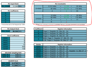
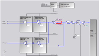
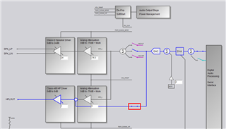
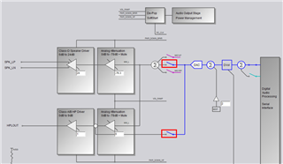
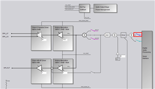
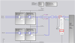
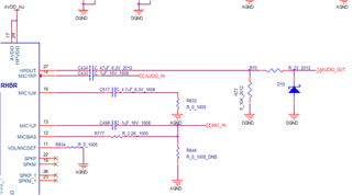
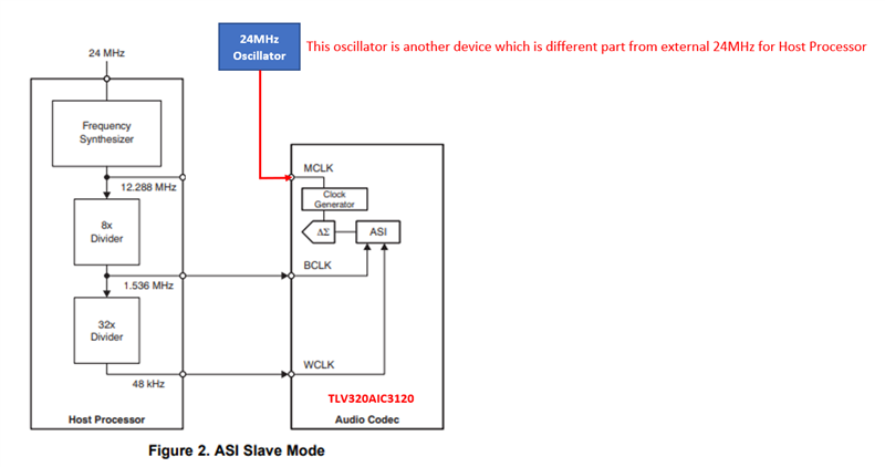
Their board is configured two board which is processor b'd and audio codec b'd.

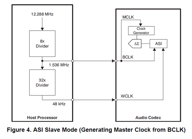
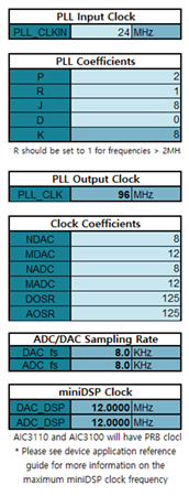
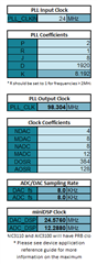
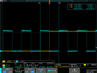
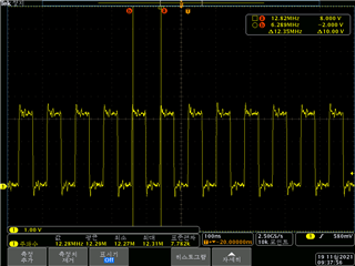
This audio codec can't receive MCLK from processor b'd.

So they have to use another clock source from another oscillator which is different from oscillator of process.

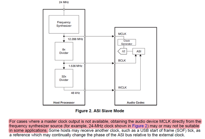
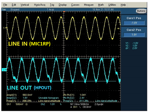
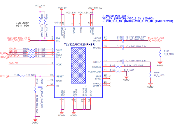
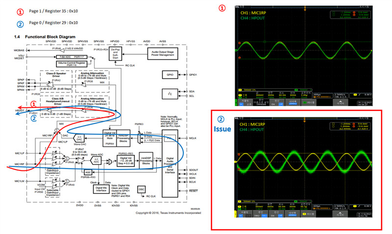
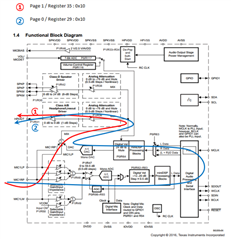
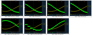
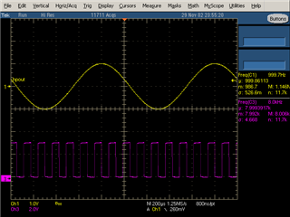
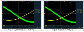
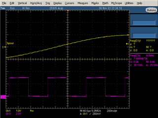
Below is their block diagram to use it.

Is there no problem? Can they use it?

Best Regards,

Michael

  • Hi Michael,

    What's the reason Codec can't receive MCLK that goes to host?

    You will need to synchronize the MCLK to host and Codec.

    Regards,

    Peter

  • Hi Peter,

    Thanks for your kind feedback.

    Their host processor can't send MCLK to audio codec.

    When I checked app. note like below, there is commented.

    Audio Serial Interface Configurations for Audio Codecs (Rev. A)

    When each part (oscillator) must be used like our customer case, can't they use audio codec?

    If they use like this case, What is your expected issue?

    Another method is like below, do they have to use BCLK? 

    Could you please give me your resolution?

    Best Regards,

    Michael

  • Hi Michael,

    For this codec, this is the clock generation tree which you can take in BCLK, just make sure the configurations meet the criteria.

    You can read more in section 7.3.13 of the datasheet.

    Regards,

    Peter

  • Hello Peter,

    Could you please send your comment to me about each above my questions?

    Below is captured.

    BR,

    Michael

  • Hi Michael,

    • No Oscillator for this part.
    • They will be out of sync.
    • Yes as explained in the clock diagram above.
    • Either use the same MCLK as host or use BCLK.

    Regards,

    Peter

  • Hi Peter,

    First of all, I want to say that thank you for your kind support.

    I have another issue and need your help.

    Our customer is evaluating that audio loopback path from MIC1RP to HPOUT.

    Signal distortion is observed on the HPOUT like below waveform.

    Could you please check symptom, schematic, register setting and give your opinion to me?

    * Symptom

    * Schematic

    * Register setting


    page:0

    Register : 1(0x01)

    data:  1(0x01)

    page:0

    Register : 30(0x1e)

    data:  1(0x01)

    page:0

    Register : 19(0x13)

    data: 12(0x0c)

    page:0

    Register : 18(0x12)

    data:  8(0x08)

    page:0

    Register : 12(0x0c)

    data: 12(0x0c)

    page:0

    Register : 11(0x0b)

    data:  8(0x08)

    page:0

    Register : 5(0x05)

    data: 33(0x21)

    page:0

    Register : 4(0x04)

    data:  3(0x03)

    page:0

    Register : 29(0x1d)

    data:  0(0x00)

    page:0

    Register : 5(0x05)

    data: 33(0x21)

    page:0

    Register : 6(0x06)

    data:  8(0x08)

    page:0

    Register : 7(0x07)

    data:  0(0x00)

    page:0

    Register : 8(0x08)

    data:  0(0x00)

    page:0

    Register : 11(0x0b)

    data:  8(0x08)

    page:0

    Register : 12(0x0c)

    data: 12(0x0c)

    page:0

    Register : 13(0x0d)

    data:  0(0x00)

    page:0

    Register : 14(0x0e)

    data:125(0x7d)

    page:0

    Register : 18(0x12)

    data:  8(0x08)

    page:0

    Register : 19(0x13)

    data: 12(0x0c)

    page:0

    Register : 20(0x14)

    data:125(0x7d)

    page:0

    Register : 30(0x1e)

    data:  1(0x01)

    page:0

    Register : 5(0x05)

    data:161(0xa1)

    page:0

    Register : 11(0x0b)

    data:136(0x88)

    page:0

    Register : 12(0x0c)

    data:140(0x8c)

    page:0

    Register : 18(0x12)

    data:136(0x88)

    page:0

    Register : 19(0x13)

    data:140(0x8c)

    page:0

    Register : 30(0x1e)

    data:129(0x81)

    page:0

    Register : 116(0x74)

    data:  0(0x00)

    page:0

    Register : 68(0x44)

    data:  0(0x00)

    page:0

    Register : 63(0x3f)

    data:148(0x94)

    page:0

    Register : 64(0x40)

    data:  4(0x04)

    page:0

    Register : 61(0x3d)

    data:  4(0x04)

    page:0

    Register : 81(0x51)

    data:128(0x80)

    page:0

    Register : 82(0x52)

    data:  0(0x00)

    page:1

    Register : 33(0x21)

    data: 78(0x4e)

    page:1

    Register : 35(0x23)

    data: 64(0x40)

    page:1

    Register : 36(0x24)

    data:  0(0x00)

    page:1

    Register : 37(0x25)

    data:  0(0x00)

    page:1

    Register : 31(0x1f)

    data:130(0x82)

    page:1

    Register : 40(0x28)

    data:  6(0x06)

    page:1

    Register : 48(0x30)

    data: 16(0x10)

    page:1

    Register : 49(0x31)

    data: 64(0x40)

    page:1

    Register : 50(0x32)

    data:  0(0x00)

    Best regards,

    Michael

  • Hi Michael,

    Try with the following settings:

    3465.register.xlsx

    based on the following clock tree.:

    regards,

    Peter

  • Hello Peter,

    I always thank you for your kind support.

    Our customer has another issue on the No.2 audio path like below image.

    No.1 audio path is no issue.

    They set all of gain 0dB on the No.2 audio path.

    But, Output is higher than the input signal and has noise.

    Could you please check register setting and give me resolution?

    Our customer have to clear this issue and produce mass product.

    Pls help us.

    * Symptom image

    * Regiser setting

    No. [page 0]   No. [page 1]
    0 reg:0x00, value:  0 (0x000) 0 reg:0x00, value:  1 (0x001)
    1 reg:0x01, value:  0 (0x000) 1 reg:0x01, value:  0 (0x000)
    2 reg:0x02, value:  1 (0x001) 2 reg:0x02, value:  0 (0x000)
    3 reg:0x03, value:102 (0x066) 3 reg:0x03, value:  0 (0x000)
    4 reg:0x04, value:  3 (0x003) 4 reg:0x04, value:  0 (0x000)
    5 reg:0x05, value:145 (0x091) 5 reg:0x05, value:  0 (0x000)
    6 reg:0x06, value:  8 (0x008) 6 reg:0x06, value:  0 (0x000)
    7 reg:0x07, value:  0 (0x000) 7 reg:0x07, value:  0 (0x000)
    8 reg:0x08, value:  0 (0x000) 8 reg:0x08, value:  0 (0x000)
    9 reg:0x09, value:  0 (0x000) 9 reg:0x09, value:  0 (0x000)
    10 reg:0x0a, value:  0 (0x000) 10 reg:0x0a, value:  0 (0x000)
    11 reg:0x0b, value:176 (0x0b0) 11 reg:0x0b, value:  0 (0x000)
    12 reg:0x0c, value:130 (0x082) 12 reg:0x0c, value:  0 (0x000)
    13 reg:0x0d, value:  0 (0x000) 13 reg:0x0d, value:  0 (0x000)
    14 reg:0x0e, value:128 (0x080) 14 reg:0x0e, value:  0 (0x000)
    15 reg:0x0f, value:128 (0x080) 15 reg:0x0f, value:  0 (0x000)
    16 reg:0x10, value: 12 (0x00c) 16 reg:0x10, value:  0 (0x000)
    17 reg:0x11, value:  0 (0x000) 17 reg:0x11, value:  0 (0x000)
    18 reg:0x12, value:176 (0x0b0) 18 reg:0x12, value:  0 (0x000)
    19 reg:0x13, value:130 (0x082) 19 reg:0x13, value:  0 (0x000)
    20 reg:0x14, value:128 (0x080) 20 reg:0x14, value:  0 (0x000)
    21 reg:0x15, value:128 (0x080) 21 reg:0x15, value:  0 (0x000)
    22 reg:0x16, value:  4 (0x004) 22 reg:0x16, value:  0 (0x000)
    23 reg:0x17, value:  0 (0x000) 23 reg:0x17, value:  0 (0x000)
    24 reg:0x18, value:  0 (0x000) 24 reg:0x18, value:  0 (0x000)
    25 reg:0x19, value:  0 (0x000) 25 reg:0x19, value:  0 (0x000)
    26 reg:0x1a, value:  1 (0x001) 26 reg:0x1a, value:  0 (0x000)
    27 reg:0x1b, value:  0 (0x000) 27 reg:0x1b, value:  0 (0x000)
    28 reg:0x1c, value:  0 (0x000) 28 reg:0x1c, value:  0 (0x000)
    29 reg:0x1d, value:  0 (0x000) 29 reg:0x1d, value:  0 (0x000)
    30 reg:0x1e, value:136 (0x088) 30 reg:0x1e, value:  0 (0x000)
    31 reg:0x1f, value:  0 (0x000) 31 reg:0x1f, value:134 (0x086)
    32 reg:0x20, value:  0 (0x000) 32 reg:0x20, value:  6 (0x006)
    33 reg:0x21, value:  0 (0x000) 33 reg:0x21, value: 78 (0x04e)
    34 reg:0x22, value:  0 (0x000) 34 reg:0x22, value:  0 (0x000)
    35 reg:0x23, value:  0 (0x000) 35 reg:0x23, value: 64 (0x040)
    36 reg:0x24, value:192 (0x0c0) 36 reg:0x24, value:  0 (0x000)
    37 reg:0x25, value:168 (0x0a8) 37 reg:0x25, value:  0 (0x000)
    38 reg:0x26, value: 17 (0x011) 38 reg:0x26, value:127 (0x07f)
    39 reg:0x27, value:  0 (0x000) 39 reg:0x27, value:127 (0x07f)
    40 reg:0x28, value:  0 (0x000) 40 reg:0x28, value:  7 (0x007)
    41 reg:0x29, value:  0 (0x000) 41 reg:0x29, value:  2 (0x002)
    42 reg:0x2a, value:  0 (0x000) 42 reg:0x2a, value:  0 (0x000)
    43 reg:0x2b, value:  0 (0x000) 43 reg:0x2b, value:  0 (0x000)
    44 reg:0x2c, value:  0 (0x000) 44 reg:0x2c, value: 32 (0x020)
    45 reg:0x2d, value:  0 (0x000) 45 reg:0x2d, value:134 (0x086)
    46 reg:0x2e, value:  0 (0x000) 46 reg:0x2e, value:  2 (0x002)
    47 reg:0x2f, value:  0 (0x000) 47 reg:0x2f, value:  0 (0x000)
    48 reg:0x30, value:  0 (0x000) 48 reg:0x30, value: 32 (0x020)
    49 reg:0x31, value:  0 (0x000) 49 reg:0x31, value:128 (0x080)
    50 reg:0x32, value:  0 (0x000) 50 reg:0x32, value:  1 (0x001)
    51 reg:0x33, value:  2 (0x002) 51 reg:0x33, value:  0 (0x000)
    52 reg:0x34, value: 50 (0x032) 52 reg:0x34, value:  0 (0x000)
    53 reg:0x35, value: 18 (0x012) 53 reg:0x35, value:  0 (0x000)
    54 reg:0x36, value:  2 (0x002) 54 reg:0x36, value:  0 (0x000)
    55 reg:0x37, value:  2 (0x002) 55 reg:0x37, value:  0 (0x000)
    56 reg:0x38, value:  2 (0x002) 56 reg:0x38, value:  0 (0x000)
    57 reg:0x39, value: 17 (0x011) 57 reg:0x39, value:  0 (0x000)
    58 reg:0x3a, value: 16 (0x010) 58 reg:0x3a, value:  0 (0x000)
    59 reg:0x3b, value:  0 (0x000) 59 reg:0x3b, value:  0 (0x000)
    60 reg:0x3c, value:  1 (0x001) 60 reg:0x3c, value:  0 (0x000)
    61 reg:0x3d, value:  4 (0x004) 61 reg:0x3d, value:  0 (0x000)
    62 reg:0x3e, value:  0 (0x000) 62 reg:0x3e, value:  0 (0x000)
    63 reg:0x3f, value:148 (0x094) 63 reg:0x3f, value:  0 (0x000)
    64 reg:0x40, value:  4 (0x004) 64 reg:0x40, value:  0 (0x000)
    65 reg:0x41, value:  0 (0x000) 65 reg:0x41, value:  0 (0x000)
    66 reg:0x42, value:  0 (0x000) 66 reg:0x42, value:  0 (0x000)
    67 reg:0x43, value:  0 (0x000) 67 reg:0x43, value:  0 (0x000)
    68 reg:0x44, value:  0 (0x000) 68 reg:0x44, value:  0 (0x000)
    69 reg:0x45, value: 56 (0x038) 69 reg:0x45, value:  0 (0x000)
    70 reg:0x46, value:  0 (0x000) 70 reg:0x46, value:  0 (0x000)
    71 reg:0x47, value:  0 (0x000) 71 reg:0x47, value:  0 (0x000)
    72 reg:0x48, value:  0 (0x000) 72 reg:0x48, value:  0 (0x000)
    73 reg:0x49, value:  0 (0x000) 73 reg:0x49, value:  0 (0x000)
    74 reg:0x4a, value:  0 (0x000) 74 reg:0x4a, value:  0 (0x000)
    75 reg:0x4b, value:238 (0x0ee) 75 reg:0x4b, value:  0 (0x000)
    76 reg:0x4c, value: 16 (0x010) 76 reg:0x4c, value:  0 (0x000)
    77 reg:0x4d, value:216 (0x0d8) 77 reg:0x4d, value:  0 (0x000)
    78 reg:0x4e, value:126 (0x07e) 78 reg:0x4e, value:  0 (0x000)
    79 reg:0x4f, value:227 (0x0e3) 79 reg:0x4f, value:  0 (0x000)
    80 reg:0x50, value:  0 (0x000) 80 reg:0x50, value:  0 (0x000)
    81 reg:0x51, value:128 (0x080) 81 reg:0x51, value:  0 (0x000)
    82 reg:0x52, value:  0 (0x000) 82 reg:0x52, value:  0 (0x000)
    83 reg:0x53, value:  0 (0x000) 83 reg:0x53, value:  0 (0x000)
    84 reg:0x54, value:  0 (0x000) 84 reg:0x54, value:  0 (0x000)
    85 reg:0x55, value:  0 (0x000) 85 reg:0x55, value:  0 (0x000)
    86 reg:0x56, value:  0 (0x000) 86 reg:0x56, value:  0 (0x000)
    87 reg:0x57, value:  0 (0x000) 87 reg:0x57, value:  0 (0x000)
    88 reg:0x58, value:127 (0x07f) 88 reg:0x58, value:  0 (0x000)
    89 reg:0x59, value:  0 (0x000) 89 reg:0x59, value:  0 (0x000)
    90 reg:0x5a, value:  0 (0x000) 90 reg:0x5a, value:  0 (0x000)
    91 reg:0x5b, value:  0 (0x000) 91 reg:0x5b, value:  0 (0x000)
    92 reg:0x5c, value:  0 (0x000) 92 reg:0x5c, value:  0 (0x000)
    93 reg:0x5d, value:  0 (0x000) 93 reg:0x5d, value:  0 (0x000)
    94 reg:0x5e, value:  0 (0x000) 94 reg:0x5e, value:  0 (0x000)
    95 reg:0x5f, value:  0 (0x000) 95 reg:0x5f, value:  0 (0x000)
    96 reg:0x60, value:  0 (0x000) 96 reg:0x60, value:  0 (0x000)
    97 reg:0x61, value:  0 (0x000) 97 reg:0x61, value:  0 (0x000)
    98 reg:0x62, value:  0 (0x000) 98 reg:0x62, value:  0 (0x000)
    99 reg:0x63, value:  0 (0x000) 99 reg:0x63, value:  0 (0x000)
    100 reg:0x64, value:  0 (0x000) 100 reg:0x64, value:  0 (0x000)
    101 reg:0x65, value:  0 (0x000) 101 reg:0x65, value:  0 (0x000)
    102 reg:0x66, value:  0 (0x000) 102 reg:0x66, value:  0 (0x000)
    103 reg:0x67, value:  0 (0x000) 103 reg:0x67, value:  0 (0x000)
    104 reg:0x68, value:  0 (0x000) 104 reg:0x68, value:  0 (0x000)
    105 reg:0x69, value:  0 (0x000) 105 reg:0x69, value:  0 (0x000)
    106 reg:0x6a, value:  0 (0x000) 106 reg:0x6a, value:  0 (0x000)
    107 reg:0x6b, value:  0 (0x000) 107 reg:0x6b, value:  0 (0x000)
    108 reg:0x6c, value:  0 (0x000) 108 reg:0x6c, value:  0 (0x000)
    109 reg:0x6d, value:  0 (0x000) 109 reg:0x6d, value:  0 (0x000)
    110 reg:0x6e, value:  0 (0x000) 110 reg:0x6e, value:  0 (0x000)
    111 reg:0x6f, value:  0 (0x000) 111 reg:0x6f, value:  0 (0x000)
    112 reg:0x70, value:  0 (0x000) 112 reg:0x70, value:  0 (0x000)
    113 reg:0x71, value:  0 (0x000) 113 reg:0x71, value:  0 (0x000)
    114 reg:0x72, value:  0 (0x000) 114 reg:0x72, value:  0 (0x000)
    115 reg:0x73, value:  0 (0x000) 115 reg:0x73, value:  0 (0x000)
    116 reg:0x74, value:  0 (0x000) 116 reg:0x74, value:  0 (0x000)
    117 reg:0x75, value: 96 (0x060) 117 reg:0x75, value:  0 (0x000)
    118 reg:0x76, value:  0 (0x000) 118 reg:0x76, value:  0 (0x000)
    119 reg:0x77, value:  0 (0x000) 119 reg:0x77, value:  0 (0x000)
    120 reg:0x78, value:  0 (0x000) 120 reg:0x78, value:  0 (0x000)
    121 reg:0x79, value:  0 (0x000) 121 reg:0x79, value:  0 (0x000)
    122 reg:0x7a, value:  0 (0x000) 122 reg:0x7a, value:  0 (0x000)
    123 reg:0x7b, value:  0 (0x000) 123 reg:0x7b, value:  0 (0x000)
    124 reg:0x7c, value:  0 (0x000) 124 reg:0x7c, value:  0 (0x000)
    125 reg:0x7d, value:  0 (0x000) 125 reg:0x7d, value:  0 (0x000)
    126 reg:0x7e, value:  0 (0x000) 126 reg:0x7e, value:  0 (0x000)
    127 reg:0x7f, value:  0 (0x000)   127 reg:0x7f, value:  0 (0x000)

    Best regards,

    Michael

  • Hi Michael,

    From the registers above, it looks like they are not following my register suggestion.

    The clock setting is based on MCLK of 24MHz and the sampling of 8KHz as shown above.

    Please ask them to try with the attached settings and the host will need to provide WCLK=8KHz and BCLK=256KHz.

    I don't know how they connect the digital data on their system, they could use the internal loopback as well.

    test2 register.xlsx

    Regards,

    Peter

  • Hi Peter,

    I'm sorry for the additional request.

    Their MCLK is 12.288MHz not 24MHz.

    Also they will set MCLK 12.288MHz finally.

    They can't change this MCLK from 12.288MHz to 24MHz.

    So I need register setting which is based on MCLK 12.288MHz.

    I'm looking forward to receiving this register.

    Pls help me again.

    Best regards,

    Michael

  • Hi Michael,

    You should be able to assist them in the future with the register settings.

    To change the MCLK, you use the PLL calculator and configure the different dividers to get the sampling rate as shown below and make sure the PLL constraints are not violated based on D value.

    I have attached the register setting per the new MCLK this time.

    test2 register 12.288MHz_MCLK.xlsx

    Regards,

    Peter

  • Hello Peter,

    We applied these register setting what you sent.

    But, test result is same.

    Also, we have test another audio path which is CPU (Digital, Sine Wave 1KHz Signal) -> Audio Codec (DAC -> HPOUT).

    When we check signal w/ scope at HPOUT, there is noise like jitter.

    Below is waveform.


    Do you have any good idea to solve it or your opnion?

    and which registers do I have to check and change?

    Could you please tell me what do I do?

    Best regards,

    Michael

  • Hi Michael,

    That should not be the case.

    Can you capture 2 periods of WCLK along with BCLK with the scope and i2cdump of the register to confirm again?

    To speed up the process, is it possible to format the registers like what I placed in the excel sheet?

    Regards,

    Peter

  • Hello Peter,

    Here is what you requested.

    I'm sorry that WCLK, BCLK waveform is not captured together on one window.

    I got these waveform individually from customer.

    It's not easy, but please check first.

    Register dump

    codec_chip_reg.xlsx

    BCLK - 256KHz

    WCLK - 8KHz

    MCLK - 12.288MHz

    Best regards,

    Michael

  • Hi Michael,

    They are NOT using the register settings I sent for the 12.288MHz above.

    Also the WCLK is not correct, that looks like the same as BCLK.

    8787.codec_chip_reg.xlsx

    Regards,

    Peter

  • Hello Peter,

    I received feedback from our customer after setting what you sent.

    But, there is no effect. Symptom is same.

    Which condition or register can make jitter noise or our customer's symptom?

    Could you please send it to me If you have any idea or check point?

    Best regards,

    Michael

  • Hello Michael,

    Peter is out of office until next week, please be patient as we continue to try to assist you during this holiday week.

    Best Regards,

    Carson

    LPA Applications Engineer

  • Hi Michael,

    There are 2 possible causes here:

    1. Either the register settings are not right or
    2. Board filter is needed

    if they are sure the settings are matching to what I have provided then the next step is to send me the schematic on the HPOUT.

    Regards,

    Peter

  • Hello Peter,

    This issue is not a register setting or board filter problem.

    I evaluated "TLV320AIC3120EVM-U" to clarify this issue.

    Finally, I observed noise from DAC of this device.

    Also I checked that this noise is added on 1KHz Sine Wave like customer issue.

    I have to send a root cause to our customer. 

    Could you please check EVM and feedback your test result to me?

    Also tell me whether this device has this fault or not.

    * Test result w/ EVM

    1. Ground noise level for reference


    2. Noise level at HPOUT.

     2-1. HPOUT noise level and test condition

     * HPOUT noise

     * Test condition

     2-2. HPOUT noise level and test condition

     * HPOUT noise

     * Test condition

     2-3. HPOUT noise level and test condition

     * HPOUT noise

     * Test condition

     2-4. HPOUT noise level and test condition

     * HPOUT noise

     * Test condition

    Best regards,

    Michael

  • Hello Peter,

    2'nd test condition image of 2-3 HPOUT noise level and test condition is not for HPOUT noise.

    In this condition, noise is same with the result of 2-2 or 2-3.

    I'm sorry for the confusion.

    Best regards,

    Michael

  • Hi Michael,

    The EVM was designed for HPOUT jack which normally connected to the headphone which has filter built in.

    So if you just monitor at this output you will see the high frequency noise.

    I have captured the HPOUT using the EVM with and without the LPF and you can see the difference.

    CH1 is after the LPF and CH2 is the output at the audio jack.

    Regards,

    Peter

  • Hi Peter,

    That sounds good news.

    I think that this issue will be cleared if you send LPF circuit (include component value).

    Could you please send it to me ASAP?

    Here is final schematic of customer.

    Best regards,

    Michael

  • Hi Michael,

    I'm using 100 Ohm and 47nF to give a cutoff about 33.8K.

    Regards,

    Peter

  • Hi Peter,

    I don't know well where do I put LPF circuit before C434 or after C434.

    Could you please give me circuit drawing from Pin27 (HPOUT) to LPF of end point?

    I'm waiting your feedback now.

    Best regards,

    Michael

  • Hi Michael,

    Swap the position of C434 and R77, change C434 to 47nF and R77 to 100Ohm.

    Regards,

    Peter

  • Hello Peter,

    I always thank you for your kind support.

    When we applied LPF at HPOUT, we observed improvement of noise.

    Test condition is No.2 path like below.

    I have two issue now.

    Could you please check and reply to me?

    1. When we zoom up the signal of output after LPF circuit, we can observe that there is stair step like below.

        Could you please tell me whether we can improve this stair step or not?

    2. They set all of gain 0dB on the No.2 audio path.

        But, Output is higher than the input signal like below.

    Register setting is what you sent.

    211201_d4216_ti_reg_setting.xlsx

    When I checked the register, I think that there is no problem.

    Could you check and reply to me what's the root cause?

    Best regards,

    Michael

  • Hi Michael,

    It seems like settings are still not correct if path 1 is good.

    Can you ask them to do an i2cdump again?

    Regards,

    Peter

  • Hi Peter,

    Excel file what I sent you like below is their setting and dump.

    0572.211201_d4216_ti_reg_setting.xlsx

    What do I have to send more to you?

    Pls let me know more specific.

    Did you test on path 2 ?

    If yes, could you please send capture image which is compared Input(MIC1RP) and Output(HPOUT after LPF)?

    Additionally, could you please send register setting file after test path 2 in condition MCLK = 12.288MHz?

    We will test with it.

    Could you tell me about my question 1?

    Best regards,

    Michael

  • Hi Michael,

    If you set the gain to 0dB but output is not reflecting that, it could be that the settings are not correct - that's why I asked to check again.

    Try this setting I highlighted in red. 

    4503.211201_d4216_ti_reg_setting.xlsx

    If it's still the same then we need to just check the path independently, check the ADC path by capturing the digital output through an audio precision or some analyzer and check against your input then if the ADC path correct then proceed with routing the ADC data to DAC path.

    Regards,

    Peter

  • Hi Peter,

    I have a question.

    When I check your register setting, what's the reason why do I do set "DIN-to-DOUT loopback is enabled"?

    We need to check "ADC-to-DAC loopback is enabled".

    If you can test w/ EVM as our customer's test condition, we can check that there is same issue or not.

    Could you first test it and let me know test result?

    This way is the best to talk with our customer about their issue.

    Pls help me.

    Best regards,

    Michael

  • Hi Peter,

    I think that you will be very busy, but I and our customer really want to find root cause of this issue.

    First of all, your test result of EVM is very important.

    So, Could you please share your test result on EVM?

    Pls refer to the below that is our additional test result.

    1.  Test for "ADC to DAC loopback of EVM"

     -. Pin2 of J2 (MIC1LP) on EVM : 1Vp-p 1khz sine wave from Function Generator (Ch1)

     -. Pin2 of J4 (HPL) on EVM : There is no output (Ch4)

        So, finally I couldn't test it on EVM.

        Pls check this and let me know.

     -. Test setup and GUI setting

    2. Test for "SoC to DAC" path.

        Compare their original B'd (Nuvoton codec, Reference set) to our codec mounted B'd.

        Test result is that HPOUT level of our codec b'd is more than Original B'd.

        So, I'm wonder whether there is issue or not on the ADC path.

    -. Original B'd (Nuvoton codec, Reference set)

    -. Our codec mounted B'd

    I'm looking forward to receiving your test result and more specific response.

    Thanks and best regards,

    Michael

  • Hi Michael,

    I'll get back to you next week.

    Regards,

    Peter

  • Hi Peter,

    Ok, I will wait and hope to get your good feedback.

    Best regards,

    Michael

  • Hi Michael,

    Here is what I see on the EVM, it shows output a little higher than the input.

    Is this a problem for customer?

    Regards,

    Peter

  • Hi Peter,

    Yes, right.

    We need to get root cause from you why this result has happened.

    I need your detail explain about this to talk with our customer.

    Additionally, I don't know why hpout can't out on my EVM test.

    Could you send your test setting on the GUI tool and EVM?

    Best regards,

    Michael

  • Hi Michael,

    This is not spec violation, the headset FS output voltage is a typical value.

    It's normal to have little variation, you can always play with the gain.

    Attached is my setting.

    AIC3120_ADC_DAC_init_0dB_for test_classD_mute.txt
    w 30 00 00
    # (c) Initiate SW Reset
    #
    w 30 01 01
    #
    # 2. Program Clock Settings
    # (a) Program PLL clock dividers P,J,D,R (if PLL is necessary)
    #
    # PLL_clkin = MCLK = 11.2896MHz, codec_clkin = PLL_CLK,
    # P=1, R=1, J=8, D=0000
    w 30 04 03
    w 30 06 08
    w 30 07 00
    w 30 08 00
    #
    # (b) Power up PLL (if PLL is necessary)
    w 30 05 91
    # (c) Program and power up NADC
    #
    # NADC = 2, divider powered on
    w 30 12 82
    #
    # (d) Program and power up MADC
    #
    # MADC = 8, divider powered on
    w 30 13 88
    #
    # (e) Program OSR value
    #
    # AOSR = 128
    w 30 14 80
    # NDAC is powered up and set to 8
    w 30 0B 88
    # MDAC is powered up and set to 2
    w 30 0C 82
    # DOSR = 128, DOSR(9:8) = 0, DOSR(7:0) = 128
    w 30 0D 00 80
    #
    # (f) Program I2S word length as required (16, 20, 24, 32 bits)
    #
    # mode is i2s, wordlength is 16, slave mode (default)
    w 30 1B 00
    # DIN to DOUT, ADC to DAC loopback
    w 30 1d 30
    #
    # (g) Program the processing block to be used
    #
    # ADC PRB_R4
    w 30 3d 04
    # select DAC DSP Processing Block PRB_P16
    w 30 3C 10
    # page 8 enable adaptive filter
    w 30 00 08
    w 30 01 04
    # page 0
    w 30 00 00
    #
    # 3. Program Analog Blocks
    # (a) Set register Page to 1
    #
    w 30 00 01
    #
    # (b) Program MICBIAS if applicable
    #
    # Programmed MICBIAS always on, 2.5V
    # w 30 2E 0A
    # Micbias = AVDD
    w 30 2e 0a
    #
    # (c) Program MicPGA
    # (d) Routing of inputs/common mode to ADC input
    # (e) Unmute analog PGAs and set analog gain
    #
    # MICPGA P = MIC1LP 20kohm
    w 30 30 80
    #
    # MICPGA M - CM 20kohm
    w 30 31 80
    #
    # Program common-mode voltage (default = 1.65 V)
    #
    w 30 1F 14
    # Program headphone-specific depop settings (in case headphone driver is used)
    #
    # De-pop, Power on = 800 ms, Step time = 4 ms
    w 30 21 4E
    #
    # Program routing of DAC output to the output amplifier (headphone/lineout or speaker)
    #
    # DAC routed to HPOUT
    w 30 23 40
    #
    # Unmute and set gain of output driver
    #
    # Unmute HPOUT, set gain = 0 db
    w 30 28 06
    # mute Class-D, set gain = 6 dB
    w 30 2A 00
    #
    # Power up output drivers
    #
    # HPOUT powered up, Vcom=1.65V
    w 30 1F 92
    # Power-down Class-D drivers
    w 30 20 06
    # Enable HPOUT output analog volume, set = 0 dB
    w 30 24 80
    # Disable Class-D output analog volume, set = -9 dB
    w 30 26 12
    # 4. Program ADC
    #
    # (a) Set register Page to 0
    #
    w 30 00 00
    #
    # (b) Power up ADC channel
    w 30 51 80
    #
    # Power up DAC channels and set digital gain
    #
    # Powerup DAC (soft step enabled)
    w 30 3F 94
    #
    # DAC gain = 0 dB
    w 30 41 00
    # (c) Unmute digital volume control and set gain
    #
    # UNMUTE ADC
    w 30 52 00
    # Unmute DAC
    w 30 40 04

    I'm closing this case now.

    Regards,

    Peter

  • Hi Peter,

    We wanted to get your explain about root cause of this issue.

    There was not enough commnet. Anyway, we will accept it.

    Below issue has been asked before.

    Could you please give a resolution to me?

    This symptom is what I have to resolve.

    Pls help.

    When we zoom up the signal of output after LPF circuit, we can observe that there is stair step like below.

    Could you please tell me whether we can improve this stair step or not?

    Best regards,

    Michael

  • Hi Michael,

    Maybe try with different sampling 44.1KHz for example and see if the same thing is seen there, I don't know their system as I don't see it with EVM.

    Regards,

    Peter

  • Hi Peter,

    Our customer has already confirmed that there is no issue at sampling rate 44.1KHz.

    But their system can support only for sampling rate 8KHz, 16KHz (G.711/ADPCM 16KHz).

    Could you please give me a solution (register setting. etc) after one more check in condition of MCLK 12.288MHz, Sampling rate 8KHz, 16KHz?

    We're almost there now, so please help a little more.

    Thanks and Best regards,

    Michael

  • Hello,

    Right now our experts are out of office until Dec. 28th due to Holidays. We will get back to your question as soon as possible when we resume operations.

    Happy Holidays

    LPA Applications Team

  • Hi Michael,

    Do they know is it from ADC or DAC path? They should check the path separately instead of blindly trying with different settings.

    Try different PRB like change the current PRB_P4 or PRB_R4 to P6 or R6, higher processing capability will consume more power.

    Regards,

    Peter

  • Hi Peter,

    Happy new year!!!

    I will try it following your guide.

    Now I want to get your register setting file what you test in condition of MCLK 12.288MHz, Sampling rate 8KHz, 16KHz.

    If it is no issue register setting file, we will test after apply it to customer b'd.

    BR,

    Michael

  • Hi Peter,

    Here is our test result.

    But there is no improvement on DAC path.

    Refer to the below test result.

    BR,

    Michael

  • Hi Michael,

    The EVM is not build for external MCLK, give me till next week to order and modify an EVM.

    In the mean time, try with 16KHz and you can also play with different DOSR.

    Regards,

    Peter

  • Hi Peter,

    Thanks and I got it.

    I will try with 16KHz and also wait your test result.

    BR,

    Michael

  • Hi Michael,

    This is my DAC settings for 8KHz and the response.

    AIC3120_DAC_init_0dB_for test_8KHz_768.txt
    # page 0 is selected 
    w 30 00 00
    # s/w reset
    > 01
    # Program Clock Settings
    # (a) Program PLL clock dividers P,J,D,R (if PLL is necessary)
    #
    # PLL_clkin = MCLK = 12.288MHz, codec_clkin = PLL_CLK,
    w 30 04 03
    # J=8, D=0000
    w 30 06 08
    w 30 07 00
    w 30 08 00
    #
    # (b) Power up PLL (if PLL is necessary and P & R value)
    # P=1, R=1,
    w 30 05 91
    # NDAC is powered up and set to 2
    w 30 0B 82
    # MDAC is powered up and set to 8
    w 30 0C 88
    # DOSR = 768, DOSR(9:8) = 11, DOSR(7:0) = 00
    w 30 0D 03 00
    #
    # (f) Program I2S word length as required (16, 20, 24, 32 bits)
    #
    # mode is i2s, wordlength is 16, slave mode (default)
    w 30 1B 00
    # select DAC DSP Processing Block PRB_P4
    w 30 3C 04
    w 30 00 08
    w 30 01 00
    w 30 00 00
    #
    # page 1 is selected
    w 30 00 01
    # Program common-mode voltage (defalut = 1.35 V)
    #
    w 30 1F 04
    # De-pop, Power on = 800 ms, Step time = 4 ms
    w 30 21 4e
    #
    # Program routing of DAC output to the output amplifier (headphone/lineout or speaker)
    #
    # DAC routed to HPOUT
    w 30 23 40
    #
    # Unmute and set gain of output driver
    #
    # Unmute HPOUT, set gain = 0 db
    w 30 28 06
    #
    # Power up output drivers
    #
    # HPOUT powered up
    w 30 1F 82
    # Enable HPOUT output analog volume, set = 0 dB
    w 30 24 80
    # 5. Power up DAC
    # (a) Set register page to 0
    #
    w 30 00 00
    # Power up DAC channels and set digital gain
    #
    # Powerup DAC (soft step enabled)
    w 30 3F 94
    #
    # DAC gain = 0 dB
    w 30 41 00
    # (c) Unmute digital volume control and set gain
    #
    # Unmute DAC
    w 30 40 00

    Regards,

    Peter

  • Hi Peter,

    Thank you very much for your effort and feedback.

    We can't find stair issue at span 400us of oscilloscope.

    We need to check waveform in condition of span (Tdiv = 40us) as our customer setting.

    So we can clarify this issue.

    Could you please check and send waveform what I requested?

    Best regards,

    Michael

  • Hi,

    Please try on their setup with this setting as I have seen improvement.

    Regards.

  • Hi Peter,

    Could you check it again in condition 40us/div, 200mV/div of oscilloscope?

    This setup was our customer's condition.

    When I check it at 40us/div, 1V/div w/ customer, there is same as you sent waveform.

    But, When I check it at 40us/div, 200mV/div, there is no improvement.

    Pls send me the captured waveform.

    Another question is about your text file.for the register setting.

    Below code is what you sent.

    Do I have to write first w 30 1F 04 and then w 30 1F 82 in order?

    1F 04 is reset value.

    Otherwise, is it possible to write w 30 1F 86 at once?

    ---------------------------------------------------------------------------

    # page 1 is selected

    w 30 00 01

    # Program common-mode voltage (defalut = 1.35 V)

    #

    w 30 1F 04

    # De-pop, Power on = 800 ms, Step time = 4 ms

    w 30 21 4e

    #


    ...


    # HPOUT powered up

    w 30 1F 82

    # Enable HPOUT output analog volume, set = 0 dB

    w 30 24 80

    # 5. Power up DAC

    # (a) Set register page to 0

    #

    ---------------------------------------------------------------------------

    Best regards,

    Michael