Because of the holidays, TI E2E™ design support forum responses will be delayed from Dec. 25 through Jan. 2. Thank you for your patience.

This thread has been locked.

If you have a related question, please click the "Ask a related question" button in the top right corner. The newly created question will be automatically linked to this question.

TAS2559: TAS2557 / TAS2559 initialization with non-standard clocking

Part Number: TAS2559
Other Parts Discussed in Thread: TAS2557, TMS320F28015, , TAS2505, TAS2563, TAS2552, TAS2555

Hi,

I am evaluating the TAS2559 in hopes of using it (or the TAS2557) to replace a Cirrus Logic/Wolfson WM9081 in an existing design. The WM9081 uses the following configuration:

  • Input clock is 15 MHz. This clock comes from a TMS320F28015, and is connected to the MCLK input of the WM9081.
  • The WM9081 divides the 15 MHz clock by 2 to generate an internal FLL reference clock of 7.5 MHz.
  • The FLL of the WM9081 is used to generate an internal CLK_SYS of 11.29 MHz.
  • The WM9081 generates BCLK of 705.62 kHz and a LRCLK of 22050 Hz. BCLK and LRCLK are outputs from the WM9081 to an FPGA.
  • The FPGA uses BCLK and LRCLK to generate a DACDAT output that goes to the WM9081.
  • The WM9081 converts the DACDAT I2S data stream from the FPGA into mono audio with a class D amp.
  • The I2C interface of the TMS320F28015 is used to configure the WM9081 and to control the volume during operation.

The TAS2557 or TAS2559 look like possible replacements for the WM9081, but configuration looks to be a problem due to our use of non-standard clocking and the limited documentation for TAS series devices. Hence the following questions:

  1. Is the TAS2557 or TAS2559 an appropriate choice? Note that we have an immediate need. Better devices that are out of stock are not a solution.
  2. Are the TAS2557 and TAS2559 pin compatible if only one I2S interface is needed?
  3. Can the PLL be configured to generate a suitable clock for a 22050 sample rate given our 15 MHz input?
  4. Is there any official documentation for the PLL? I see that another user managed to reverse engineer a portion of the PLL (tas2559 pll and clocking configuration). (I have to say that it's pretty disappointing that he had to do that.)
  5. Assuming the PLL can be used to generate 11.29 MHz from 15 MHz, what are the PLL constraints that need to be observed (VCO Fmax, Fmin, etc.)?

Note that while many of the DSP features of these devices look very interesting, our immediate need is for I2S to mono audio out to a 4 ohm speaker. We would be using ROM Mode 1 for the foreseeable future.

Currently I have a TAS2559EVM here and I was hoping to be able to tack some wires onto our existing WM9081 board in order to try out the TAS2559, but PPC3 seems very limited in terms of clocking configuration. At this point it seems I'd be better off just poking registers over I2C, but I don't want to head down that path without knowing that the TAS2557 or TAS2559 will do what I want.

Thanks for your help.

galen

  • Hi Galen,

    There may be some previous e2e threads with related information. Specifically based on this one I have the below information: https://e2e.ti.com/support/audio-group/audio/f/audio-forum/801728/tas2557-initialization---22050hz-16bit/2966982#2966982

    Attached is a script I tested using a clock generator to feed 15MHz and get back BCLK ~= 705.6kHz and WCLK ~= 22.05kHz from TAS2557. This is not an audio 15MHz source so I cannot test audio playback, but clocks are being output correctly from TAS2557.
    The relevant commands to configure the device clock as output and the dividers is at the very end of the script.
    This script is based on a ROM Mode 2 - 44.1kHz configuration (multiple of 22.05kHz), so you can do similarly with other modes using the same base.

    combined_configuration_0_ROMMode2_44.1KHz_MODIFIED.cfg

    Best regards,
    -Ivan Salazar
    Applications Engineer

  • Thanks for the the config file. I was able to load it into my TAS2559EVM. I initially got a WCLK of 8.8 kHz. Looking at the config file I found that WDIV was set to 80. I changed this to 32 in order to get the desired 22.05 kHz WCLK.

    I suspect I will have more questions about this config, but this is a good start. In the meantime, could you please answer my other questions (1, 2, and 4) if you have time? Thanks.

  • Hi Galen,

    Good to hear you can use the script.
    Regarding those specific questions:

    1. TAS2557 or TAS2559 are OK, if higher power is required you may consider newer devices like TAS2563. Or if looking for a simpler device TAS2505 may be an option, although this is lower power output compared to TAS255x or TAS2563 (no integrated boost)

    2. Yes, TAS2557 and TAS2559 are pin to pin compatible if used as mono only.

    4. Unfortunately no further documentation is readily available for these devices.

    Best regards,
    -Ivan Salazar
    Applications Engineer

  • Hi,

    After connecting the TAS2559EVM to my hardware(MCLK and DIN to EVM, BCLK and WCLK from EVM, common GND), and using the config you supplied (with WDIV changed to 32), the TAS2559 is generating BCLK=706 kHz, WCLK=22.05 kHz. However, when my system sends non-zero sample data over DIN, all I get is noise. If the TAS2559 gain is high enough, the TAS2559 clocks stop, so I guess at least the TAS2559 protection is working.

    Any thoughts on what might be wrong, or how I should go about finding the problem?

  • Also, I discovered that my old Wolfson design actually supports two different MCLK frequencies, 15 MHz as mentioned above, and 1.875 Mhz (15 / 8). We changed to the lower frequency to reduce EMI. Could you please regenerate the TAS2559 config file for a MCLK input of 1.875 MHz. Alternatively, please let me know the constraints on the PLL such that I can calculate the values for myself (reference freq min/max, VCO freq min/max, etc.).

    thanks,

    galen

  • Hi Galen,

    Perhaps there is format mismatch between TAS2559 and the host.
    Can you share more details on how is the host I2S interface configured? Is it I2S, RJF, LJF or other? Any offset bits?
    Is the noise reduced or eliminated when playing at lower volume levels?

    Best regards,
    -Ivan Salazar
    Applications Engineer

  • Hi,

    I think I have fixed the noise issue. It was a signal integrity issue. I have flying wires between my board and the EVM. I shortened the connections for MCLK and DIN, and I added an additional GND. That seems to have cleaned things up.

    Regarding the PLL settings, here is the situation. My existing design derives its sample rate by dividing 60 MHz by 2721, which gives ~22050.72. Changing this sample rate is not an option, so I am trying to match it as closely as possible. Currently I driving the TAS2559 with a 1.875 MHz MCLK. I am using the following settings for the PLL:

    w 98 00 00	# select page 0
    w 98 7f 00	# select book 0
    w 98 00 01	# select page 1
    w 98 73 0f	# NDIV_MUX_CLKIN input is from PLL_CLK
    w 98 74 0d	# PLL_CLKIN input is from GPI2
    w 98 00 00	# select page 0
    w 98 7f 64	# select book 100
    w 98 1b 01	# TAS2559_PLL_P_VAL_REG
    w 98 1c 1e	# TAS2559_PLL_J_VAL_REG
    w 98 1d 06	# TAS2559_PLL_D_VAL_MSB_REG (6 bits right justified)
    w 98 1e d2	# TAS2559_PLL_D_VAL_LSB_REG (8 bits)
    w 98 20 02	# TAS2559_PLL_N_VAL_REG
    w 98 22 08	# ?
    w 98 02 10	# ?
    w 98 21 08	# TAS2559_DAC_MADC_VAL_REG
    w 98 01 08	# TAS2559_DAC_INTERPOL_REG
    w 98 2b 00	# TAS2559_RAMP_CLK_DIV_MSB_REG
    w 98 2c 40	# TAS2559_RAMP_CLK_DIV_LSB_REG
    w 98 1f 20	# TAS2559_CLK_MISC_REG
    w 98 2a 00	# TAS2559_ISENSE_DIV_REG
    

    Do the same PLL rules apply to the TAS2559 as to the TAS2552 as described in SLAA892? If so, I'm violating the minimum PLL_CLKIN frequency when D != 0. When I tried setting P=0 and dividing J.D by 2, the TAS2559 did not generate BCLK and WCLK. It is unclear to me why this did not work. Please advise.

    It's unclear to me what frequencies are needed by the various internal clocks, particularly those associated with the DSP. Initially I plan to use ROM mode 1 or 2, but at some point in the future we may want to use the more advanced features. What's the best approach to generating a working config, preferably one that doesn't require a lot of hand-holding here on the forum? I've tried a few times to generate configs using PPC3, but it seems to generate large configs that write to many mystery registers, where it's not clear whether those registers are even relevant in the ROM modes. And of course there's the issue of PPC3 not support non-standard MCLK frequencies.

    thanks,

    galen

  • Hi Galen,

    Glad to hear it was just signal integrity issue.

    I found some old documents about clock distribution on these long released devices (TAS2555/7/9).
    Let me go through these and give you further comments by the end of the week.

    Best regards,
    -Ivan Salazar
    Applications Engineer

  • Hello again,

    My config seems to be mostly working now, although I have no idea whether I'm using the device within spec, for obvious reasons. Nonetheless, today I edited the config file to remove everything that looked like it wasn't relevant for mode 1 operation. The end result is the attached file. It still contains some mystery register writes which I found were required. My latest stumbling block is volume control. I've tried writing to B0P60R112-115 as shown in the Digital Volume Control app note that you created, but writing to these registers does not appear to have any effect. Is there some other register that controls whether the R112-R115 gain control is active?

    tas2559_mode1_simple.cfg

  • Hi Galen,

    I'll review the cfg and let you know if there is anything outstanding after cross reference with the internal clock tree documentation.

    Regarding volume control, I think the registers mentioned in the document are only enabled in tuning mode, although you may be able to use a different set of registers controlling amplifier level on the analog side instead; I'll also include some more details on this later.

    Best regards,
    -Ivan Salazar
    Applications Engineer

  • Hi,

    We are in the process of designing in the TAS2559. If possible, can you please respond to these three items?

    1. What are the correct values for the PLL registers, given a 1.875 MHz MCLK and a desired WCLK output of 22050.72 Hz (60 MHz / 2721), and a desired BCLK output of 705622.9 Hz (WCLK * 32)? See my previous message.
    2. Can you please confirm that the Digital Volume Control function associated with registers B0P60R112-115 is not available in ROM Mode 1 or 2?
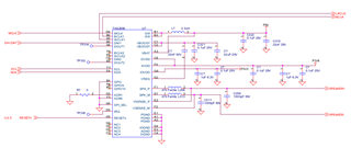
    3. Can you please do a quick review of the following schematic?

    Thanks!

  • Hi Galen,

    I'll review your questions and come back early next week. Sorry for the late response.

    Best regards,
    -Ivan Salazar
    Applications Engineer

  • Hi,

    Sorry to bother you about this, but I would still like to get these questions answered, particularly the PLL question.

    thanks,

    galen

  • Hi Galen,

    Given this uncommon clock frequencies and ratios, it gets very complicated to calculate the whole clock tree settings. I tried to focus on DAC_MOD_CLK as well as BCLK and WCLK outputs from BDIV and WDIV:

    • DAC_MOD_CLK should be 64*FS, based on your settings it would seem like it is something like ~160*FS
    • BDIV output seems close to 705622.9Hz, being ~707217.188
    • WDIV output seems too low by a factor of ~4 being ~8840.21Hz

    I'll reach out over private message to share some more details on the internal clocks, but I would suggest to change the system for better known clocks if possible.

    Digital Vol Ctrl from B0P60R112-115 is not available in ROM mode, as those registers are part of the DSP memory (not used in ROM mode). You may try with B0P0R6 Bits 6-3 (do not change this value in SmartAmp mode, use only in ROM mode).

    Best regards,
    -Ivan Salazar
    Applications Engineer

  • The DAC_MOD_CLK setting comes from the original configuration that you attached in your first response, where BDIV is set to 5. I was just copying that. I believe my clock settings are as follows:

    • WDIV = 32
    • BDIV = 5
    • MDIV = 8
    • NDIV = 2
    • J.D = 30.106567  (30 + 1746 / 16384)
    • P = 1
    • reference frequency = 1.875 MHz

    My limited understanding of the clock tree suggests that this would generate a sample rate of 11025, but the actual sample rate is 22050, which is what I need. If there are constraints on the internal clocks (PLL, DSP, DAC_MOD) and the ratios between them, it would be very helpful to know them. Other than the unexplained factor of 2, I think I know which registers control the various dividers. I just need to know the constraints that must be maintained.

    thanks,

    galen

  • Hi Galen,

    Ivan is out of office until Monday OCT 17, please wait until he comments or continues the thread.

    Thank you for your patience.

    Kind Regards,

  • Hi Galen,

    I reached out through private message to share further details.
    Just to better understand the current situation: With the clock configurations you have, is your application able to play sound?

    Best regards,
    -Ivan Salazar
    Applications Engineer