This thread has been locked.

If you have a related question, please click the "Ask a related question" button in the top right corner. The newly created question will be automatically linked to this question.

PCM3168A: In 16K TDM mode, DOUT1 has no output

Part Number: PCM3168A

Hi Team,

SPI configuration:

reg:0x40, value:0xC1

reg:0x41, value:0x07

reg:0x50, value:0x01

reg:0x51, value:0x07
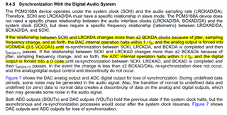
Clock Status:

LRCKAD (purple): 16KHZ BCKAD (blue): 4.096MHZ SCKI (yellow): 4.096MHZ DOUT1 (bottom blue): no output

  • Did you provide signals unto the ADC inputs? How about the DAC output, does it work when you stream data to the DAC?

    Regards.

  • Hi Pdjuandi,

    Input audio from VIN6+ VIN6- two analog pins, but DOUT1 has no output. The DAC also doesn't work, but ZERO's feet are responsive. 

    If the data input through DIN1 is not 0, ZERO will be pulled low.

    If the data input through DIN1 is 0, ZERO is pulled high.

    It seems that the digital part works fine (spi read and write is normal), but the analog part doesn't work at all (analog input and output have no signal). Is there any way to check it?

    Thanks,

    Annie

  • This could be caused by SCKI and LRCLK relation as described in section 9.4.5 in the datasheet, can you check that if everything else is fine like supply or RST signal etc.?

    Do you see this on all devices? Can you trigger on DOUT just to make sure?

  • Hi Pdjuandi,

    Not found from SCKI and LRCLK as described in Section 9.4.5, jitter occurs or the switching error of LRCKDA is greater than 2BCKDA. The following is the voltage status of some pins

    VCOMAD,2.141,
    AGNDAD2,0,
    VCCAD2,4.83,
    RST,3.3,V
    OVF,3.29,V
    LRCKD,16,KHZ
    BCKAD,4.096,MHZ
    DOUT1,0,V
    DOUT2,0,V
    DOUT3,0,V
    DGND2,0,V
    VDD2,3.29,V
    ZERO,0,V
    VCCDA1,4.84,V
    VCOMDA,2.42,V
    AGNDDA1,0,V
    VOUT8+,2.41,V
    VOUT8-,2.41,V
    VOUT7+,2.41,V
    VOUT7-,2.41,V
    VOUT6+,2.41,V
    VOUT6-,2.41,V
    VOUT5+,2.41,V
    VOUT5-,2.41,V
    VOUT4+,2.41,V
    VOUT4-,2.41,V
    VOUT3+,2.41,V
    VOUT3-,2.41,V
    VOUT2+,2.41,V
    VOUT2-,2.41,V
    VOUT1+,2.41,V
    VOUT2-,2.41,V
    AGMDDA2,0,V
    VCCDA2,4.83,V
    LRCKDA,16,KHZ
    BCKDA,4.096,MHZ
    DIN1,0,V
    DIN2,0,V

    Please help to check if there is any obvious problem with the pin status? Only one board is made, so there is no other equipment to compare.

    Use a logic analyzer to analyze SCLK LRCKDA BCKDA DIN, it can be parsed normally. Although the logic analyzer shows that the protocol is correct, there is no way to judge whether the SCLK and LRCLK synchronization of the chip is normal.

    Thanks,

    Annie

  • Hi Annie,

    Our audio expert, Peter is out of office until next week, please wait until he returns and comments to continue the thread.

    Thank you for your patience

  • Hi,

    It looks like there's an issue with the synchronization as VOUT = VCOMDA.

    Try triggering on SCKI and check LRCLK/BCLK if they are jittery.

    Regards.

  • Hi Pdjuandi,

    Try triggering on SCKI

    Customer would like to know how to trigger on SCKI? Disconnect LRCLK from BCLK, only let SCKI output the signal, and then observe LRCLK/BCLK?

    Thanks,

    Annie

  • Set the scope to trigger SCKI and monitor LRCLK/BCLK.