This thread has been locked.

If you have a related question, please click the "Ask a related question" button in the top right corner. The newly created question will be automatically linked to this question.

TAS6584-Q1: Communication and timing during LOAD DIAG state

Expert 4640 points
Part Number: TAS6584-Q1

Dear e2e support,

In Figure 8-1, there is this timing diagram:

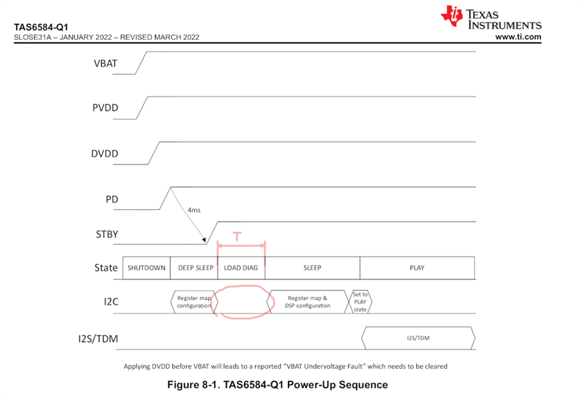
During the LOAD DIAG state, no communication is made to i2c. This raises some questions:

  • Does TAS ignores all communication during that state?
  • If I ask TAS for a state change during LOAD DIAG, is it latched and will it be applied at the end, or is it just ignored?
  • Assuming each channel has one speaker connected, how long can the LOAD DIAG state last?

Regards,

  • Hi, 

    Please see below my comments.

    • Does TAS ignores all communication during that state?

             No, device can not ignore any communication during DC diag.

    • If I ask TAS for a state change during LOAD DIAG, is it latched and will it be applied at the end, or is it just ignored?

                You can abort DC diag by register 0xB0.

    • Assuming each channel has one speaker connected, how long can the LOAD DIAG state last?

              If loads no error, 4 channels will cost 155ms typical time to finish DC diag.

  • Hi Yanming,

    Thank you for your responses, I have two more questions about this topic

    1) I tried various load configurations to see how much time does it take to do the load diagnosis:

    - with all the channels connected the time is around 150 ms as you said

    - with channel 1 disconnected it takes around 300 ms, whether the other channels are disconnect or not

    - with one or more channels disconnected between channels 2, 3 and 4 it takes around 250 ms

    Is it normal this asymmetry between the channels? 

    2) At the startup the first thing I do is rising up the PD pin and programming the TAS registers with the I2C. While doing some analyses i noticed this:

    https://i.postimg.cc/7LgMJrFH/Microsoft-Teams-image.png

    The first five times the microcontroller tryes to write the TAS registers it fails despite the PD been fully up, then after those attempts the connection works as it should. Is there a reason for that? Should we wait some time after whe PD is up before programming the TAS?

  • Hi Marco,

    1) Once load has error, DC diag will repeat again to double confirm the error, so it will cost more time. You test looks make sense.

    2) Sorry, I can not open your picture. You can insert picture directly into E2E.

    Regards,

    Derek

  • Hi Marco,

    I think device was running DC diag after PD was pull high. Automatic DC load diagnostics at device initialization cannot be bypassed but can be aborted by setting bit 0 and bit 7 in DC LDG Ctrl 1 Register (Address = 0xB0) to ‘1’ if desired.

    You can try to set bit 7 in DC LDG Ctrl 1 Register (Address = 0xB0) to ‘1’ and then send I2C comments again.

    Regards,

    Derek

  • The STBY pin was down so the TAS should be in DEEP SLEEP state after the rising of PD and not in LOAD DIAG as I see from the image at the beginning of this post.

    Anyway to be more specific I have 4 TAS in my design, I program them in the same way but this problem doesn't occur to the first TAS, it happens only for the other three.

    Regards,

    Marco

  • Hi Marco,

    Could you share your schematic and script code at first to us?

    Let me check if any error or mistakes.

  • Unfortunately I'm not allowed to share neither the schematic or the code.

    We continued to investigate on the issue and we noticed that the only difference between the TAS in the schematic is the resistance used for the I2C address.

    It seems that TAS with a resistance different from 0ohm (either pullup or pulldown) take at least 180us after the PD is raised before starting to communicate with I2C. The TAS with a 0ohm resistance instead is ready after less than 40us.

    Does this make any sense to you? Is it possible that the I2C address resistor value influences the time before the TAS is ready to communicate?

  • I have similar question.

    see  this

    best regards

  • Hi Cialdi,

    Thank you!

    Let me double confirm it.

  • Hi Cialdi,

    Shadow's comments make sense. When PD is pull high, digital reset still cost some time, and then internal detection and comparator will latch I2C address.

    As confirmed with design team, 200us is safe time after PD is high and I2C communication is normal. 

    Regards,

    Derek

  • Shadow's comments make sense. When PD is pull high, digital reset still cost some time, and then internal detection and comparator will latch I2C address.

    As confirmed with design team, 200us is safe time after PD is high and I2C communication is normal. 

    Shadow has stated that "they" suggest to wait 10ms.

    take a look here:

    Shadow said:

    Speaking of power on sequence, we suggest to wait 10ms after pull up PDN pins, and then start other operation. Not only the address deteciton you mentioned, there's also other LDO need time to be fully ready.

    I don't know who "they" refers to.

    You say you talked to the design team and they confirm that 200us is enough. Shadow says 10ms is better instead. Did he talk to the same design team you talked to?

    So is 200us enough or do you need 10ms?

  • Hi Cialdi,

    I think Shadow means power sequence requirement. After PD is high, delay at least 4ms to pull STBY to high.

    200us is minimum time of I2C response. 

    When STBY is low, analog logic is reset, and configure I2C address can not trigger ananlog logic work. So Shadow suggest that  it is better to wait 4ms to configure I2C when PD is high.

    Regards,

    Derek

  • Hi

    We measured the register write at about 5ms (i2c @400kHz) and we have 4 TAS on our board.
    So about 20ms in total. Adding 4ms for each TAS we have 36ms.
    In any case we raise STBY after register programming (and after an additional wait). So it is guaranteed that between PDn raised and STBY raised there is more than 4ms.
    So the question is: Is it reliable and safe to program the registers after 200us from raising PDn, but before 4ms? What drawbacks are there?

    In other words, we want to minimize the time between PDn raised and STBY raised (obviously not less than 4ms) and for this reason we start writing registers as soon as possible (after 200us from PDn raised, as you told us). How safe and reliable is this?

    regards

  • Hi Cialdi,

    Understood! Thank you!

    200us is simulation data in device side from design team. It does not consider the IO delay related to pull_up/down through resistor, althogh the delay is very low.

    I think 200us is safe theoretically. It is better to evaluate on your boards and check several boards to have almost same time delay.

    Regards,

    Derek

  • ok, thank you,

    since we have an RTOS with tick at 1ms, the minimum wait to guarantee the 200us is between 1 and 2 ms, so we are comfortable.

    regards

    Max

  • Hi Cialdi,

    That's fine.

    If you have no other questions, I will close the E2E.

    Please contact with me if you need any help.

    Regards,

    Derek

  • ok to close

    regards

    Max