This thread has been locked.

If you have a related question, please click the "Ask a related question" button in the top right corner. The newly created question will be automatically linked to this question.

TLV320ADC3100: TLV320ADC3100

Part Number: TLV320ADC3100
Other Parts Discussed in Thread: TLV320ADC3120

Hi, 

We are using the TLV320ADC3100 audio codec for our project. We write in the register first, and then we verify it by reading the registers. However, the value we get after reading the register is different from what we wrote there. Is there anything we have to take care for I2C peripheral? 

We have configured the Audio codec in master mode and our desire output is:

BCLK: 2.8224Mhz

WCLK: 44.1khz

Sample Size: 32-bit

For that we have given the MCLK of 12.288Mhz.

Also, below are the configured register's value.


ADC310X_PAGE_SELECT - 0x00 // Page - 0 selected

ADC310X_RESET - 0x01 // Soft Reset

ADC310X_CLK_GEN_MUX - 0x00 // Clock Generation

ADC310X_PLL_PR_VAL - 0x91 // PLL_CLK - 90.3168 

ADC310X_PLL_J_VAL - 0x07 // J - 7

ADC310X_PLL_D_VAL_MSB - 0x0D // 

ADC310X_PLL_D_VAL_LSB - 0xAC // Combination of MSB and LSB is 3500 for D

ADC310X_NADC_CLK - 0x88 // NADC - 8 

ADC310X_MADC_CLK - 0x82 // MADC - 2 as per our calculations

ADC310X_AOSR - 0x80 // Oversampling - 128

ADC310X_ADC_IADC - 0x20 // IADC - 32

ADC310X_ADC_INTF_CTRL_1 - 0x3C // i2s for adc interface with 32 bits sample size, both BCLK and WCLK as output 

ADC310X_ADC_INTF_CTRL_2 - 0x06 // BDIV_CLKIN = ADC_CLK and both are active even with the codec powered down

ADC310X_BLCK_N_DIV - 0x82 // Value is 2 as per our calculations.

ADC310X_ADC_PROC_BLK- 0x01 // ADC signal processing block PRB_R1

ADC310X_PAGE_SELECT - 0x01 // Page - 1 selected

ADC310X_PGA_ANALOG_L - 0x00 // Left PGA gain = 0 dB and muted

ADC310X_PGA_ANALOG_R - 0x00 // Right PGA gain = 0 dB and muted

ADC310X_INPUT_SEL_PGA_L_1 - 0xfc // Left ADC Input selection for Left PGA = IN1L(P) as Single-Ended

ADC310X_INPUT_SEL_PGA_R_1 - 0xfc // Right ADC Input selection for Right PGA = IN1R(M) as Single-Ended

ADC310X_PAGE_SELECT - 0x00 Page - 2 selected.

ADC310X_ADC_DIGITAL - 0xc2 // Power-up Left ADC and Right ADC

ADC310X_ADC_VOL_CTRL - 0x00 // Unmute digital volume control and set gain = 0 dB

Please suggest some suggestions.

Thanks & Regards 

Lakshita

  • Are you not able to read any register correct?

  • Helllo Sanjay, 

    The issue of the register is solved. Thanks for the help. 

    But currently we are configuring the codec in master mode. But the desire clock is not generated from the codec.

    Below are the register configurations:

    Desired : WCLK - 44.1kHz, BCLK - 2.8224Mhz

    Given clock from external source : MCLK - 12Mhz

    ADC310X_PAGE_SELECT - 0x00 // Page - 0 selected
    ADC310X_RESET - 0x01 // Soft Reset
    ADC310X_CLK_GEN_MUX - 0x00 // Clock Generation
    ADC310X_PLL_PR_VAL - 0x91 // PLL_CLK - 90.3168 
    ADC310X_PLL_J_VAL - 0x07 // J - 7
    ADC310X_PLL_D_VAL_MSB - 0x14 
    ADC310X_PLL_D_VAL_LSB - 0x90 // Combination of MSB and LSB is 5264 for D
    ADC310X_PLL_PR_VAL - 0x91 // Again as per the datasheet
    ADC310X_NADC_CLK - 0x88 // NADC - 8 
    ADC310X_MADC_CLK - 0x82 // MADC - 2 as per our calculations
    ADC310X_AOSR - 0x80 Oversampling - 128
    ADC310X_ADC_IADC - 0x20 // IADC - 32
    ADC310X_ADC_INTF_CTRL_1 - 0x3c // i2s for adc interface with 32 bits sample size, both BCLK and WCLK as output 
    ADC310X_ADC_INTF_CTRL_2 - 0x03 // BDIV_CLKIN = ADC_MOD_CLK (generated on-chip)
    ADC310X_BLCK_N_DIV-  0x82 // Value is 2 as per our calculations
    ADC310X_ADC_PROC_BLK - 0x01 // ADC signal processing block PRB_R1
    ADC310X_PAGE_SELECT - 0x01 Page - 1 selected
    ADC310X_MIC_BIAS_CTRL - 0x60 // Mic biasing for 3v3
    ADC310X_PGA_ANALOG_L - 0x00 // Left PGA gain = 0 dB and muted
    ADC310X_PGA_ANALOG_R - 0x00 // Right PGA gain = 0 dB and muted
    ADC310X_INPUT_SEL_PGA_L_1 - 0xfc // Left ADC Input selection for Left PGA = IN1L(P) as Single-Ended
    ADC310X_INPUT_SEL_PGA_R_1 - 0xfc // Right ADC Input selection for Right PGA = IN1R(M) as Single-Ended
    ADC310X_PAGE_SELECT - 0x00 // Page - 2 selected.
    ADC310X_ADC_DIGITAL - 0xc2 // Power-up Left ADC and Right ADC
    ADC310X_ADC_VOL_CTRL - 0x00 // Unmute digital volume control and set gain = 0 dB

    We have used TI provided excel sheet for the calculations.

    We have taken the case which is highlighted above in the image.

    Please suggest some solutions regarding it.

    Thanks

    Lakshita

  • Before we looked into the PLL Setup i wanted to ask if you have seem the TLV320ADC3120 Chip? It is a much newer device and is supported by the Pure Path Console 3 Software which is very easy to set up

  • Hi Sanjay,

    I appreciate your recommendation. However, the custom board with the TLV320adc3100 audio codec has already been made. And we're going to stick with it.
    The clock that is produced by the register settings that I have already discussed:
    WCLK - 5.28kHz and BCLK - 338Khz

    Thanks

    Lakshita

  • Hello Sanjay,

    Thanks for your recommendation. We have checked TLV320ADC3120 but for now we won't be able to use the same in our design due to pin compatibility issues in our existing design. Can we have a call to discuss few things related to the issues we are facing in TLV320ADC3100IRGET? We can have a joint debug session as well.

    Please let us know the best time to have a call as per your availability.

  • I shall take a look at your settings and revert back shortly. After that we can look at having a call.

  • Hello Sanjay. Have you looked upon the settings? can we have a short call. This technical issue is stretching the project timeline drastically. Awaiting for your response.

  • 0250.Audio Codec.pdf

    Schematic pdf for your reference.

  • The schematic seems ok.

    The Below setting on I2C should apply for achieving the output desired

    For MCLK = 12 MHz, fS = 44.1 kHz, NADC = 8, MADC = 2, and AOSR = 128: Select P = 1, R = 1, K = 7.5264, which results in J = 7, D = 5264

    Can you recheck the I2C Values for D=5264  ? Are they not 0x29 and 0x10?

  • Hi Sanjay,

    Thanks for your valuable response. we were able to get the desired clock by Disabling the internal PLL. We are unable to get the Data from MIC. we are using single ended MIC currently and we are getting white noise only.

    We have referred the same example mentioned in the datasheet. Below are the configurations for your reference.

    ADC310X_PAGE_SELECT - 0x00 // Page - 0 selected
    ADC310X_RESET - 0x01 // Soft Reset
    ADC310X_CLK_GEN_MUX - 0x00 // Clock Generation
    ADC310X_PLL_PR_VAL - 0x11// PLL disable
    ADC310X_PLL_J_VAL - 0x04 // J - 4
    ADC310X_PLL_D_VAL_MSB - 0x00 
    ADC310X_PLL_D_VAL_LSB - 0x00
    ADC310X_NADC_CLK - 0x86 // NADC - 6 
    ADC310X_MADC_CLK - 0x82 // MADC - 2 
    ADC310X_AOSR - 0x80 // Oversampling - 128
    ADC310X_ADC_INTF_CTRL_1 - 0x30 // i2s for adc interface with 32 bits sample size, both BCLK and WCLK as input 

    ADC310X_ADC_PROC_BLK - 0x01 // ADC signal processing block PRB_R1
    ADC310X_PAGE_SELECT - 0x01 / Page - 1 selected
    ADC310X_PGA_ANALOG_L - 0x00 // Left PGA gain = 0 dB and muted
    ADC310X_PGA_ANALOG_R - 0x00 // Right PGA gain = 0 dB and muted
    ADC310X_INPUT_SEL_PGA_L_1 - 0xA0 // Left ADC Input selection for Left PGA = IN1L(P) as Single-Ended

    ADC310X_INPUT_SEL_PGA_L_2 - 0x28 // All Left and right PGA disable for differential 
    ADC310X_INPUT_SEL_PGA_R_1 - 0xA8

    ADC310X_INPUT_SEL_PGA_R_2 - 0x28
    ADC310X_PAGE_SELECT - 0x00 // Page - 2 selected.
    ADC310X_ADC_DIGITAL - 0x82 // Power-up Left ADC and Right ADC
    ADC310X_ADC_VOL_CTRL - 0x08 // Unmute digital volume control and set gain = 0 dB

    Attached is the white noise audio file. Please let us know your thoughts on the same and also if we are missing something to be implemented.


  • What Kind of Mic is used? Is it a electret condenseer Mic? Have you switched on the MicBias Voltage to power the mic?

    Can you put an oscilloscope probe on mic terminal with scope on DC Coupling. Then play a 1k tone from You tube through your mobile phone keeping the phone very close to the Mic. The scope should show the 1k on a DC Bias

  • We are using MEMS Mic. Part Number is AMM-4038-B

  • Do you see the waveform with the Oscilloscope on the mic terminal as suggested?

  • Hello Sanjay. 

    We have tried doing the same thing and we are getting the signal as suggested on MIC Output but after connecting the same with audio codec, its getting noisy and we are unable to see any such precise signal after connecting the mic output (Either differential or single ended) to the Audio Codec.

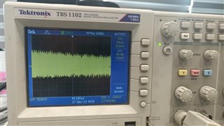
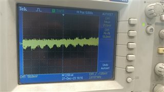
    One more thing we have noticed is while giving the MCLK From external clock generator, the MIC Input lines of audio codec pick the noise and hence there's no such data we get as per the expectations. Both the reference images elaborate on how we get the noisy lines on Audio codec while giving external MCLK.

     .

    We are getting noise on IN2L(P) and IN3L(M) Pins without even connecting these pins to MIC Outputs.

    Please let us know your thoughts on the same.

  • Some questions:

    Is the IOVDD of the Chip at 1.8V? I see the coil mounted on the schematic and thats why i ask. if this is 1.8V then you need to drive a 1.8V Level MCLK to the clk pin. You can do so through a 47 ohm resistor.

    The Noise you seen may be due to ground bounce that happens when the fast clock is connected to the chip. Where does the MCLK signal come from?

    Can you also let me know the DC Level on the input pins of the ADC?

    Do you have access to an analog audio signal generator? Would it be possible to get a 1v /1Khz sine wave Input? This can be connected direct to the ADC instead of the Mic to see if you get digital data

  • Hi Sanjay,

    Is the IOVDD of the Chip at 1.8V? I see the coil mounted on the schematic and thats why i ask. if this is 1.8V then you need to drive a 1.8V Level MCLK to the clk pin. You can do so through a 47 ohm resistor. - Yes its working on 1.8VDC.

    The Noise you seen may be due to ground bounce that happens when the fast clock is connected to the chip. Where does the MCLK signal come from? - We are generating MCLK from signal generator as well as from ESP Module. We re getting noise in both the cases.

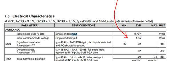
    Can you also let me know the DC Level on the input pins of the ADC? - Its 1.2VDC when not connected with MIC Output.

    Do you have access to an analog audio signal generator? Would it be possible to get a 1v /1Khz sine wave Input? This can be connected direct to the ADC instead of the Mic to see if you get digital data - Yeah we can do this and let you know the results.

  • You should connect the MCLK through a 47 ohm series resistor to the signal generator output. Please tie the ground connection of the signal cablevery close to the Chip ground.

    Then connect a 0.7V RMS /1K signal through a 1u coupling capaitor to input pin.

    The DC Voltage on the input pins should be 1.35V without any signal connected.

    1.2V seems very low