This thread has been locked.

If you have a related question, please click the "Ask a related question" button in the top right corner. The newly created question will be automatically linked to this question.

TAS2559: Product is not meeting the datasheet performance, even when measured on the EVM (also, continued PPC3/SmartAmp thermal characterization problems)

Part Number: TAS2559
Other Parts Discussed in Thread: TAS2563, TAS2555

Tool/software:

Team, 

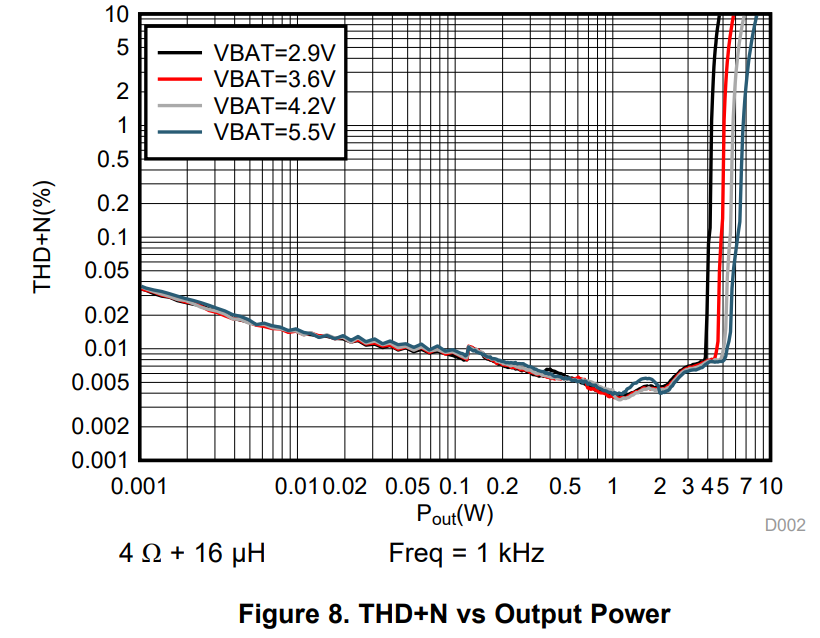
We are using the TAS2559 device in a client's design (AI-enabled Wifi/BT Smart Speaker for consumer electronic product). Here is the datasheet plot to which I am referring:


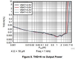
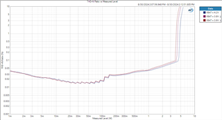
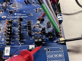
The TAS2559 EVM is not reaching the performance shown above but instead the output becomes clipped as the boost converter output sags at a much lower amplitude. This is true even if we use a DC power supply on VBATT instead of the LiIon battery.  We are clipping heavily at only 4.2W (ish). Please see images below.

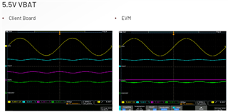
At customary LiIon battery voltages, we cannot reach rated power with a 4ohm load nor produce the performance plots shown in the datasheet on the EVM. The issue becomes less noticeable if we change the VBAT level to the maximum of 5.5V. You can see this behavior in the attached scope captures. With that in mind, here are our questions:


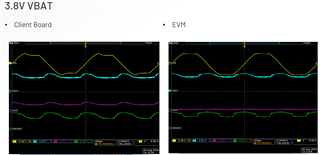
  1. Was the EVM used to create the data sheet plots (or was it done on the Characterization/Validation board which may have different construction and components)?
    1. If the former, why is it that our EVM is unable to meet the spec
    2. If the latter, can you please provide the schematic of the TAS2559 section as implemented on the Char/Validation board?
  2. We would like to de-couple the boost converter and the amplifier to test them independently to find out what's happening.
    1. Can the boost converter be loaded with an external load at the VBOOST net if the amplifier is put in High-Z mode?
    2. If not, can a load be placed on the VBOOST net while the amplifier is operating without any load (or a really high impedance load)?
    3. Can we power the Vboost net externally to test whether or not it's the amplifier that is having issues?
  3. Can we set the TAS2559 to boost to a fixed voltage (say, 6.5VDC with no Class G / Class H modulation) and the amplifier section to operate in pass through mode (i.e. no limiting, no DRC, no Smart Amp, no attenuation or other signal processing)?
    1. We are unsure if there may be something else happening- either in the data path of the audio amplifier section or in the configuration of the boost converter limits. 
    2. If that isn't the default config coming out of start-up, could you please provide an I2C config file that does this things?

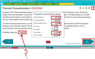
Thermal Characterization Failing.

  1. Another unrelated problem is that the speaker characterization process in PPC3 does not work for our speaker. We've read in various posts and in the SmartAmp Tuning Documentation that the speaker may be too large to get it to heat up enough to register in the PPC3 tool. In the older PPC3 plug in for the TAS2563 there was specific mention of changing the excitation signal from 16kHz to something lower to get the speaker to heat up effectively. However, the latest version of PPC3 seems to have removed that feature. How can we get it back? ... or in some other way change the excitation frequency?


  2. We read a recommendation on e2e that one could use the onboard speakers of the EVM to, in essence, trick the tool into having some values just to get the tool to progress through the rest of the characterization. I think this isn't a viable solution- afterall, we'd be configuring the SmartAmp algorithms to treat our 3W speaker like it's a 500mW microspeaker... We've also seen in this thread (https://e2e.ti.com/support/audio-group/audio/f/audio-forum/1353576/tas2563ybgevm-dc-learning-board-not-passing-audio-checks) that the tool is flakey and should be restarted/powercycled/unplugged/plugged/etc. We have done that several times to no avail.
    1. Can we perhaps use a newer device's PPC3 Plug-In, just to extract the thermal characteristics of the speaker and extract them manually?
    2. Any other ideas?

We are currently gating the client's DV build with these issues, so we'd really appreciate a quick response to help get us unstuck. If a zoom call would be easier, please PM me and I can set that up. 

  • Hi Cody,

    Good to hear from you using TI Audio.
    I assume you're testing in ROM mode, is that correct?
    I'll double check the performance on EVM on my side, in the meantime will check for any other test platform design and check for differences.

    Regarding the characterization process, the option to adjust the excitation tone was introduced for later released devices, that's why we don't see that on TAS2559 GUI. You should be able to use a new platform like TAS2563 to run the speaker characterization, and then import the char data into TAS2559.

    Best regards,
    -Ivan Salazar
    Applications Engineer

  • Hi Cody,

    I replicated the test using EVM (only OUT1 connected to 4Ohm+33uH load). You should get >3W @ <1%THD+N.

    • I removed the jumper on J2 and supplied VBAT directly to the bottom pin. The rest of the EVM powered from 5V barrel jack adapter.
    • Using the below version of PPC3 and TAS2559 app:
    • Test sequence:
      • Connect 4Ohm+33uH load to OUT1+/OUT1-
      • Connect USB from EVM to PC
      • Power 5V barrel jack
      • Power VBAT on J2-VBAT1 bottom pin
      • Enable input clocks from AP
      • Open PPC3 -> TAS2559
      • System checks -> Quit
      • Test and measurement -> ROM Mode 1
      • Device ready to test

    Hope this helps, let us know if there's any questions.

    Best regards,
    -Ivan Salazar
    Applications Engineer

  • Hi Ivan, 

    Yes, we were testing with ROM.

    Your test correlates with ours- it is nice to have reassurance that it is indeed a problem with the EVM. 


    The plot in the data sheet indicates we should be able to reach 5W before clipping. Please see Figure 8 in the data sheet. 

    Please read my original query- one of my questions is whether or not the EVM was used to create those plots in the DS... it seems it wasn't, right? So, where did those plots come from- the characterization/test board? If so, how is the schematic for that design different than the EVM? Or are there design guidelines for the boost converter that we can use to beef up the boost supply?

  • Hi Cody,

    I thought I read something about less than 3W on your post, but I see you're seeing clipping at ~4.2W.

    I'll look for the test platform used for data sheet numbers. My initial guess is that decoupling capacitors will have an impact.

    Best regards,
    -Ivan Salazar
    Applications Engineer

  • Hi Ivan, 

    Any word here? We have added ≥22uF to both VBAT and VBOOST, and that offered only 100-150mW of improvement in output power before clipping. 

    We've since tested with the TAS2563 and it is able to reach the higher power level. This design is already finalized and since the TAS2563 is not P2P compatible, we cannot exchange it for the TAS2559 currently in the design.

    Are there any other PPC3 settings or device register configurations that may be causing this?

    We appreciate your prompt responses, as the client is waiting on our findings with this issue. Can you please tell us where this plot came from? And, if it was from a TAS2559 with different external components, Can you please let us know what components were used to create this plot? Was it even the TAS2559 device?

  • Hi Cody,

    I also tried different inductor, capacitors and load connection location, no improvement so far.
    Still trying to get time from design/validation team to look into this. Will keep you posted.

    Best regards,
    -Ivan Salazar
    Applications Engineer

  • Hi Ivan,

    We really need to get this wrapped up today. Can you check with tech docs to see where the plots came from for the DS? As an alternative, whoever is doing your PCB design should be able to provide the Altium source files for the validation/characterization board so that you can see if there are any discrepancies between it and the EVM.

    In the meantime, what value Inductor did you use in your follow up testing?

  • Also, one other quick question, where can we find the original guiding documents/ design equations for how to design the boost converter for a given power range. Unless I’m missing it the data sheet assumes that everyone will simply copy and paste the application circuit but we should have the design equations documented somewhere so that we can determine what the correct value should be and compare them with the EVM.

  • Hi Ivan, checking in here. Any updates you can pass along?

  • Hi Cody,

    Checking with rest of the team tomorrow. The only other thing mentioned in documentation (old) is D2S filter, also checking if that could be the cause of distortion difference.

    Best regards,
    -Ivan Salazar
    Applications Engineer

  • It would be really helpful if we could simply find where the data sheet plot came from. If it’s not from the 2559 at all then there may perhaps be no reason to pursue this performance level. If it is Indeed from the 2559, but from a different bit of hardware, we need to find out what hardware would use to create the plot and then look for differences.

    Have you already confirmed that the plot in the data sheet was not from the 2559?

  • Cody,

    I've got confirmation that data sheet plots use LSR board (aka D2S filter). This is used for THD measurement on TAS2555/57/59/60, however D2S filter requirement is only for measurement and doesn't mean acoustic THD is affected.

    Best regards,
    -Ivan Salazar
    Applications Engineer

  • Hi Ivan, 

    LSR and D2S are internal TI acronyms, I assume? Can you please define what those are? Are these the same as the learning board filter? ... or the AUX25 filter on the Audio Precision? or ?

    If we're saying that whoever took the data sheet plots just added some additional filtering to the measurement, that could be the root cause- but it seems unlikely that this could result in the early onset of clipping, right? I suppose that, since we are trying to delineate between what is 0.3% distortion and 10% distortion, with only the resolution afforded to us in the datasheet plot.

    Can you confirm that is the only difference in test set-up?

  • Cody,

    This is referred to in Figure 18: https://www.ti.com/lit/ds/symlink/tas2559.pdf#page=16&zoom=0,0,500

    That was the result of internal discussion.

    Best regards,
    -Ivan Salazar
    Applications Engineer

  • Got it, thanks.

    So there are no other differences then? And data sheet plots were taken on the EVM but adding this circuit externally?

    If not, and if it was a characterization/validation board- can you please share those files with us so that we can understand the differences?

  • Cody,

    Correct, only mention of additional hardware is LSR board.
    No other hardware variations or files.

    Best regards,
    -Ivan Salazar
    Applications Engineer

  • Got it, thanks Ivan!