This thread has been locked.

If you have a related question, please click the "Ask a related question" button in the top right corner. The newly created question will be automatically linked to this question.

TAC5212EVM-K: How to disable the PLL?

Part Number: TAC5212EVM-K
Other Parts Discussed in Thread: TAC5212

Tool/software:

Hi all,

Because my application is a very low power one, I would like to get rid of the PLL of the TAC5212.

My requirements are:

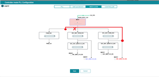
- TAC5212 shall be configured as a controller

- TAC5212 shall accept a clock of 14,745,600-Hz as CCLK

- TAC5212 shall generate FSYNC = 19,200-Hz and BCLK = 1,228,800-Hz

- TAC5212 shall transmit/receive two 32-bits words of data in I2S mode

- Internal PLL of TAC5212 shall be disabled

The ratios are:

R1 = BCLK/FSYNC = 64, R2 = CCLK/FSYNC = 768

To try to fulfill those requirements, I did the following actions:

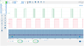
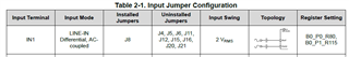
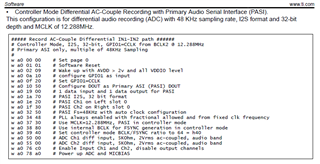
1) As a baseline, run the I2C commands (refer to the picture below) found in the EVM User's Guide, apply a clock (CCLK) of 12,288,000-Hz to GPIO1 and monitor the FSYNC signal with a scope.

I measure: FSYNC = 48,000-Hz as expected.

2) Modify the register 0x32 of page 0: set PASI_SAMP_RATE = 27d = 19,200-Hz. Then modify CCLK to 14,745,600-Hz.

I measure FSYNC = 23,040-Hz. This value was expected too because 14,745,600/12,288,000 = 1.2 thus 19,200*1.2 = 23,040-Hz.

3) Modify the register 0x32 of page 0: set PASI_SAMP_RATE = 28d = 16,000-Hz because 19,200/1.2 = 16,000-Hz.

I measure FSYNC = 19,200-Hz. At this point the generated clocks are correct.

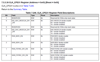
4) Check the status by reading the register 0x3E of page 0.

I read PLL_MODE_STS = 0d = PLL used in integer mode.

5) Modify the register 0x34 of page 0: set PLL_DIS = 1d = PLL is disabled, set AUTO_PLL_FR_ALLOW = 0d = PLL fractional mode disabled.

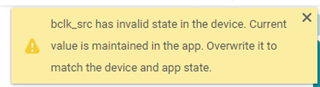
After the modification, there is no signal on FSYNC.

My question: should I modify others registers after disabling the PLL? Is there an application note describing how to get rid of the PLL?

Thanks in advance for your support.

BR,

Sébastien

  • Hi Sebastien,

    I believe since you are using 14.7456MHz CCLK (as MCLK), this is not one of the supported MCLK frequencies for automatic clocking setup in controller mode. The possible frequencies are set with the CNT_CLK_CFG2 register, and are 12, 12,288, 13, 16, 19.2, 19.68, 24, and 24.576 MHz. 

    Another note is that the device is unable to recognize the sample rate of 19.2kHz in "automatic mode", which is how it detects clocks and determines if it can disable the PLL automatically or not. If you were in target mode, to use this sample rate you would need to manually configure the PLL. I'll need to do some more testing to see if configuring the PLL and clocking dividers manually would allow you to "disable" the PLL, by setting J.D to 1.0, but I think for these clocks it would not be possible. 

    I am having trouble testing this setup on an EVM because the MCLK was not one of the allowed frequencies, and then when I changed MCLK to 12MHz for example (with a MCLK-FSYNC ratio of 625), the clocks that were output were incorrect because that FSYNC frequency is not an allowed ratio without manually setting the PLL.

    Let me know what you are able to change about your setup, or if you need these clocks, I can help you manually configure the PLL. 

    The most recent clocking configuring app note can be found here: https://www.ti.com/lit/an/slaaeg6a/slaaeg6a.pdf  I am writing an app note on manual PLL configuration that will be out in the next few months. I hope this resource helps you understand the different clocking schemes of the device.

    Best,
    Mir

  • Hello Mir,

    Thanks a lot for your support. If there is no blocking point, I would prefer to keep those clocks and to try to find out a working configuration.

    According to the application note https://www.ti.com/lit/an/slaaeg6a/slaaeg6a.pdf, I understand that it is not possible to use the automatic modes described in chapter 3 because:

    - No "Auto Primary/Secondary BCLK Ratio" because the sampling frequency of FSYNC (19,200-Hz) is not equal to one of the frequencies listed in the table 2-1.

    - No "Auto MCLK Ratio" because the PLL shall be disabled.

    - No "Auto MCLK Fixed" because the frequency of CCLK (14,745,600-Hz) is not equal to one of the frequencies listed in the table Table 3-7.

    Thus, according to chapter 3.5, we should enable the custom mode by setting the register 0x32 of page 0 to: CUSTOM_CLK_CFG = 1d = Custom clock configuration.

    Then, start the complex work! I enter the following values in page 3:

    Address Dec Address Hex Name Value Bin Value Hex Description
    d50 0x18 CLK_CFG12 b00001000 0x08 PDIV_CLKSRC_SEL=PASI BCLK, PASI_BCLK_DIV_CLK_SEL=CCLK
    d51 0x33 CLK_CFG13 b00000000 0x00 SASI_BCLK_DIV_CLK_SEL=SASI BCLK
    d52 0x34 CLK_CFG14 b10100000 0xA0 DIG_NM_DIV_CLK_SRC_SEL=CCLK, ANA_NM_DIV_CLK_SRC=DIG NM Divider
    d53 0x35 CLK_CFG15 b00000001 0x01 PLL_DIV=d1=b00000001
    d54 0x36 CLK_CFG16 b00000000 0x00 PLL_JMUL_MSB=d1=b000000001, PLL_DIV_CLK_DIG_BY_2=No divide/2, PLL_DMUL_MSB=d0=b00000000000000
    d55 0x37 CLK_CFG17 b00000000 0x00 PLL_DMUL_LSB=d0=b00000000000000
    d56 0x38 CLK_CFG18 b00000001 0x01 PLL_JMUL_LSB=d8=b000000001
    d57 0x39 CLK_CFG19 b00101000 0x28 NDIV=d1=b001, PDM_DIV=d2=b010
    d58 0x3A CLK_CFG20 b00000100 0x04 MDIV=d1=b000001, DIG_ADC_MODCLK_DIV=1
    d59 0x3B CLK_CFG21 b00000000 0x00 DIG_DAC_MODCLK_DIV=1, PASI_BDIV_MSB=d12=b00001100, SASI_BDIV_MSB=d0=b000000000
    d60 0x3C CLK_CFG22 b01000000 0x0C PASI_BDIV_LSB=d12=b000001100
    d61 0x3D CLK_CFG23 b00000001 0x01 SASI_BDIV_LSB=d1=b000000001
    d62 0x3E CLK_CFG24 b00000001 0x01 ANA_NM_DIV=d1=b000001
    d63 0x3F CLK_CFG25 b00000000 0x00 ANA_ADC_DEM_DIV=0, ANA_DAC_DEM_DIV=0
               
    d68 0x44 CLK_CFG30 b00000111 0x07 NDIV_EN=enabled, MDIV_EN=enabled, PDM_DIV_EN=enabled
    d69 0x45 CLK_CFG31 b01011111 0x5F DIG_ADC_MODCLK_DIV_EN=enabled, DIG_DAC_MODCLK_DIV_EN=enabled, PASI_BDIV_EN=enabled, SASI_BDIV_EN=enabled, PASI_FSYNC_DIV_EN=enabled, SASI_FYNC_DIV_EN=enabled
    d70 0x46 CLK_OUT_CFG1 b00000011 0x03 CLKOUT_CLK_SEL=CCLK
    d71 0x47 CLK_OUT_CFG2 b10000001 0x81 CLKOUT_DIV_EN=enabled, CLKOUT_DIV=d1=b0000001

    Note: Register 0x3F of page 3 (CLK_CFG25) is not described in the datasheet. Thus I set it to 0x00.

    In registers 0x3B and 0x3C, PASI_BDIV = 12 because CCLK/BCLK = 14,745,600-Hz / 1,228,800-Hz = 12.

    I measure: BCLK = 1,288,800-Hz and FSYNC = 19,200-Hz. Correct!

    Then I check the PLL status by reading the register 0x3E of page 0. I get: PLLMODE_STS = 2d = PLL not used. Correct!

    I configure GPIO2 as CLK_OUT and I measure 14,745,600-Hz as expected.

    Last thing: GPO1 is configured as PDMCLK (refer to the picture below) but there is no signal. I expect: 14,745,600/4 = 3,686,400-Hz.

    Are the values of the registers described above correct?

    Why no PDMCLK signal is generated?

    Futhermore, I am currently working on the clock distribution of our future device. Is it possible to send me a draft of your application note on manual PLL configuration as soon as possible please?

    BR,

    Sébastien

  • Hi,

    I'm having trouble testing your system. Can you attach your full I2C command script? The PDMCLK signal may be incorrectly divided, causing a PDM clock error that you are not aware of. Can you check the CLK_ERR_STS0 register? Also, I see that you set the PDM divider in CLK_CFG19 to be 4, so this means that the output of the PLL (that is off) is being divided by 4 to get the PDM clock. In the registers, the PDM clock is configurable to one of four options with register CNT_CLK_CFG0 in page 0:
    0d = PDM_CLK is 2.8224 MHz or 3.072 MHz
    1d = PDM_CLK is 1.4112 MHz or 1.536 MHz
    2d = PDM_CLK is 705.6 kHz or 768 kHz
    3d = PDM_CLK is 5.6448 MHz or 6.144 MHz

    These are multiples of the device being in 44.1 or 48k mode from the internal clocks. I am not sure if the PDM clock can be different than these, but maybe it can be and there would be an allowed range. If we need, I can ask the designers. What is your desired PDM clock rate? I will be able to better understand your clock tree once I have the full I2C script from you and can run it on my board.

    Also, the app note will not be ready for several months, I don't really have a good draft to send here. I am happy to help with explanations of the clock tree as needed here. You have a great start for sure.

    Best,
    Mir

  • Hi,

    Thank you to reply so fast.

    First of all, according to the datasheet, page 16, we have:

    Thus it seems to be possible to generate a PDMCLK with a frequency between 0.768-MHz and 6.144-MHz, and not necessary a multiple of 44.1-kHz or 48-kHz.

    Concerning the desired PDMCLK frequency, it should be between 1-MHz and 4-MHz.

    Below the I2C script:

    w a0 00 00 #page 0
    w a0 01 01 #reset
    w a0 02 09
    w a0 03 00
    w a0 04 00
    w a0 05 14
    w a0 06 55
    w a0 07 00
    w a0 0a 10
    w a0 0b b1
    w a0 0c 41
    w a0 0d 02
    w a0 0e 00
    w a0 0f 20
    w a0 10 51
    w a0 11 80
    w a0 12 00
    w a0 13 03
    w a0 14 00
    w a0 15 00
    w a0 18 40
    w a0 19 00
    w a0 1a 40
    w a0 1b 06
    w a0 1c 00
    w a0 1d 00
    w a0 1e 20
    w a0 1f 21
    w a0 20 30
    w a0 21 51
    w a0 22 04
    w a0 23 05
    w a0 24 06
    w a0 25 07
    w a0 26 60
    w a0 27 00
    w a0 28 20
    w a0 29 21
    w a0 2a 30
    w a0 2b 31
    w a0 2c 04
    w a0 2d 05
    w a0 2e 06
    w a0 2f 07
    w a0 32 01
    w a0 33 00
    w a0 34 c0
    w a0 35 00
    w a0 36 00
    w a0 37 30
    w a0 38 80
    w a0 39 40
    w a0 3a 00
    w a0 3b 00
    w a0 42 00
    w a0 43 50
    w a0 4b 00
    w a0 4c 5c
    w a0 4d 00
    w a0 4e 00
    w a0 4f 00
    w a0 50 00
    w a0 51 00
    w a0 52 a1
    w a0 53 80
    w a0 54 00
    w a0 55 00
    w a0 57 a1
    w a0 58 80
    w a0 59 00
    w a0 5a 00
    w a0 5b a1
    w a0 5c 80
    w a0 5d 00
    w a0 5e 00
    w a0 5f a1
    w a0 60 80
    w a0 61 00
    w a0 62 00
    w a0 64 24
    w a0 65 20
    w a0 66 20
    w a0 67 c9
    w a0 68 80
    w a0 69 c9
    w a0 6a 80
    w a0 6b 24
    w a0 6c 20
    w a0 6d 20
    w a0 6e c9
    w a0 6f 80
    w a0 70 c9
    w a0 71 80
    w a0 72 18
    w a0 73 18
    w a0 76 ef
    w a0 77 00
    w a0 78 e0
    w a0 00 01 #page 1
    w a0 0d 04
    w a0 00 03 #page 3
    w a0 32 28
    w a0 33 00
    w a0 34 a0
    w a0 35 01
    w a0 36 00
    w a0 37 00
    w a0 38 01
    w a0 39 28
    w a0 3a 04
    w a0 3b 00
    w a0 3c 0c
    w a0 3d 01
    w a0 3e 01
    w a0 3f 00
    w a0 44 07
    w a0 45 5f
    w a0 46 00
    w a0 47 81

    Below some screenshots of the setting, especially the clock configuration:

    PASI is in Controller Mode, BCLK/FSYNC ratio = 64 because 1,228,800-Hz / 19,200-Hz = 64

    MCLK (=CCLK) => CLK_VCO => CLK_SYS, the PLL is disabled

    Default values are used.

    CLK_SYS is divided by 1, then divided by 4, then drives PDM_CLK (=PDMCLK)

    CLK_SYS is divided by 1 to drive DSP_CLK, then DSP_CLK is divided by 12 because 14,745,600-Hz / 1,228,800-Hz = 12, then drives PASI BCLK

    CLKOUT_DIV is set to 1, SASI keep default values

    No error is reported in the status registers. PLL is disabled as expected.

    I measure:

    FSYNC = 19,200-Hz Correct!

    BCLK = 1,228,800-Hz Correct!

    PDMCLK (GPO1) = no signal Incorrect!

    Then, I measure CLKOUT (GPIO2) with different sources:

    If CLK_OUT_SEL=PLL output, I measure 14,745,600-Hz Correct!

    If CLK_OUT_SEL=PASI BCLK, I measure 614,400-Hz Incorrect! because 1,228,800-Hz was expected

    If CLK_OUT_SEL=SASI BCLK output, no signal Correct!

    If CLK_OUT_SEL=CCLK, I measure 7,372,800-Hz Incorrect! because 14,745,600-Hz was expected

    If CLK_OUT_SEL=internal oscillator, I measure about 6.18-MHz No idea if it is correct or not because the datasheet does not mention the frequency of the internal oscillator

    If CLK_OUT_SEL=DSP_CLK, I measure 14,745,600-Hz Correct!

    Now my questions:

    1. Why is the PDMCLK not generated?

    2. How to explain the frequencies measured on CLK_OUT? It seems that a hidden divide-by-2 is sometime added.

    Note: When the I2C script is executed, an error message is displayed but I do not know how to correct this error (refer to the picture below).

    BR,

    Sébastien

  • Hi Sebastien,

    Sorry, I will need to do some more testing and I didn't have time to go to the lab today. Something to note is that some of the PLL dividers in the PPC GUI do not enable the divider (as defined in register CLK_CFG_30 for example). So, if you run your I2C script which enables all the dividers you need, that will work better than setting some things in PPC manually and some things via the script. PDMCLK not being generated makes me think either the PDM_DIV_EN is not enabled, or the setting is not possible to be generated by the device. Going through your script, it looks like you do enable the divider and you set it to 4, which should lead to a PDM clock of 3.686MHz which is within the range that is specified for the device, but I wonder if it is not possible for it to make that clock. I will ask the designer who worked on the clocking scheme about this and get back to you with his response. 

    Also, I got the same error message. I think maybe we are setting BCLK to CCLK twice somewhere. I am not sure what the issue is but if you are getting correct clocks out I don't think it is something to worry about. 

    The hidden divide by 2 on CLK_OUT is interesting... I see you set it to have the CLKOUT divider enabled and set to 1, can you change that to disabled? Set register 0x47 on page 3 to 0x01 and see if that fixes your issue. Also, for all these issues, make sure you measure after running your script but NOT changing the GUI settings, just to make sure that any bugs with the GUI do not mess up your settings. 

    A way to check if the clock dividers are on is to read from the registers that set the enable/disable for the dividers. So, please try to read from PDM_DIV_EN and make sure that that is on.

    Let me know what you find from this and I will let you know about the PDMCLK as soon as I find out. 

    Best,
    Mir

  • Hi,

    I confirm you that all measures were done after executing the script, and reading back the register 0x44 of page (CLK_CFG30) gives me 0x07 meaning that PDM_DIV_EN is set to 1 then enabled.

    If I set the register 0x47 of page 3 (CLK_OUT_CFG2) to 0x01, there is no signal on GPIO2 (CLKOUT) whatever the sources. Thus it seems that disabling the divider disables the CLKOUT output.

    Today I modified the frequency of CCLK applied to GPIO1 from 14,745,600-Hz to 12,288,000-Hz in order to generate standard audio frequencies.

    I measure:

    - BCLK = 1,024,000-Hz Correct! because 12,288,000-Hz / 12 = 1,024,000-Hz

    - FSYNC = 16,000-Hz Correct! because 1,024,000-Hz / 64 = 16,000-Hz

    - PDMCLK = no signal Incorrect! because 12,288,000-Hz / 4 = 3,072,000-Hz was expected and 3,072,000-Hz is one the possible frequency described in CNT_CLK_CFG0 of page 0.

    Then, I measure CLKOUT (GPIO2) with different sources:

    If CLK_OUT_SEL=PLL output, I measure 12,288,000-Hz Correct!

    If CLK_OUT_SEL=PASI BCLK, I measure 512,000-Hz Incorrect! because 1,024,000-Hz was expected

    If CLK_OUT_SEL=SASI BCLK output, no signal Correct!

    If CLK_OUT_SEL=CCLK, I measure 6,144,000-Hz Incorrect! because 12,288,000-Hz was expected

    If CLK_OUT_SEL=internal oscillator, I measure about 6.18-MHz No idea if it is correct or not because the datasheet does not mention the frequency of the internal oscillator

    If CLK_OUT_SEL=DSP_CLK, I measure 12,288,000-Hz Correct!

    Thus it seems that the "hidden" divide-by-2 is still present.

    All those measurements show that the issue with the PDMCLK seems to be not related with the master clock frequency (CCLK). Furthermore, it seems to be not related with the fact that the frequency of PDMCLK belongs to one frequency listed in the register CNT_CLK_CFG0 of page 0 or not.

    Now my questions:

    1. It seems that the divider shall be enabled in order to output a signal. Thus is it possible that there is a typo (wrong register address or bit) in the datasheet concerning the parameter PDM_DIV_EN?

    2. Can you confirm me that the PDMCLK can be generated if the PLL is disabled?

    BR,

    Sébastien

  • Hi again,

    In the datasheet, register 0x45 of page 3 (CLK_CFG31) is defined as follows:

    In PPC3, we have:

    Thus there are differences for bit 5 and bit 7.

    By modifying the register 0x45 of page 3 (CLK_CFG31) from 0x5F to 0xDF (bit 7 DIG_ADC_DEM_DIV_EN = 1), I measure 3,686,400-Hz on PDMCLK Correct! because 14,745,600-Hz / 4 = 3,686,400-Hz.

    The bit 5 DIG_DAC_DEMOD_DIV_EN has no impact to PDMCLK. Thus PPC3 should be corrected to:

    And, of course, the datasheet should be updated accordingly.

    In my script, I will replace "w a0 45 5f" with "w a0 45 ff" to be sure that all dividers are enabled.

    This solves the issue with PDMCLK. But the "hidden" divide-by-2 is still present and is still unsolved or/and unexplained.

    BR,

    Sébastien

  • Hi Sebastien,

    Thanks for your update. I discussed your situation with other engineers and we think likely the device expects the ADC to be on to enable PDM, and if the ADC DEM clock is not enabled, then the ADC cannot be on. This would be a normal use case for the PDM clock. This is a good note and I have asked our designer about it! Thanks for uncovering this as well as the difference in the register map. Those registers should probably not be hidden in the datasheet.

    As for the divide by two issue, I can test in the lab tomorrow (or if you want to, you can test) what happens if you set the device to be in target mode, where you give it a BCLK and FSYNC. I wonder if the division happens on the GPIO output then as well... I have asked our designer if he knows anything about this.

    Can you attach the code that you are using to test the CLKOUT settings so we can test with the same setup as you?

    Best,
    Mir

  • Hi,

    To verify the CLKOUT behavior, execute the following I2C commands.

    w a0 00 00 #page 0
    w a0 01 01 #reset
    w a0 02 09
    w a0 03 00
    w a0 04 00
    w a0 05 14
    w a0 06 55
    w a0 07 00
    w a0 0a 10
    w a0 0b b1
    w a0 0c 41
    w a0 0d 02
    w a0 0e 00
    w a0 0f 20
    w a0 10 51
    w a0 11 80
    w a0 12 00
    w a0 13 03
    w a0 14 00
    w a0 15 00
    w a0 18 40
    w a0 19 00
    w a0 1a 40
    w a0 1b 06
    w a0 1c 00
    w a0 1d 00
    w a0 1e 20
    w a0 1f 21
    w a0 20 30
    w a0 21 51
    w a0 22 04
    w a0 23 05
    w a0 24 06
    w a0 25 07
    w a0 26 60
    w a0 27 00
    w a0 28 20
    w a0 29 21
    w a0 2a 30
    w a0 2b 31
    w a0 2c 04
    w a0 2d 05
    w a0 2e 06
    w a0 2f 07
    w a0 32 01
    w a0 33 00
    w a0 34 c0
    w a0 35 00
    w a0 36 00
    w a0 37 30
    w a0 38 80
    w a0 39 40
    w a0 3a 00
    w a0 3b 00
    w a0 42 00
    w a0 43 50
    w a0 4b 00
    w a0 4c 5c
    w a0 4d 00
    w a0 4e 00
    w a0 4f 00
    w a0 50 00
    w a0 51 00
    w a0 52 a1
    w a0 53 80
    w a0 54 00
    w a0 55 00
    w a0 57 a1
    w a0 58 80
    w a0 59 00
    w a0 5a 00
    w a0 5b a1
    w a0 5c 80
    w a0 5d 00
    w a0 5e 00
    w a0 5f a1
    w a0 60 80
    w a0 61 00
    w a0 62 00
    w a0 64 24
    w a0 65 20
    w a0 66 20
    w a0 67 c9
    w a0 68 80
    w a0 69 c9
    w a0 6a 80
    w a0 6b 24
    w a0 6c 20
    w a0 6d 20
    w a0 6e c9
    w a0 6f 80
    w a0 70 c9
    w a0 71 80
    w a0 72 18
    w a0 73 18
    w a0 76 ef
    w a0 77 00
    w a0 78 e0
    w a0 00 01 #page 1
    w a0 0d 04
    w a0 00 03 #page 3
    w a0 32 28
    w a0 33 00
    w a0 34 a0
    w a0 35 01
    w a0 36 00
    w a0 37 00
    w a0 38 01
    w a0 39 28
    w a0 3a 04
    w a0 3b 00
    w a0 3c 0c
    w a0 3d 01
    w a0 3e 01
    w a0 3f 00
    w a0 44 07
    w a0 45 ff
    w a0 46 00
    w a0 47 81

    Then, to select the source of CLKOUT, just update the register 0x46 of page 3 (CLKOUT_CFG1) and set CLKOUT_CLK_SEL to 0, 1, 2, 3, 4 or 5.

    Connect a scope to GPIO2 to measure the frequency.

    On my side, I will not spend more time on this CLKOUT issue. I let you to come back to me as soon as you have an explanation.

    ---------------------------

    Now I execute my I2C commands (CFG1) and I apply an analog signal, 500-Hz, 0.5-Vrms, to IN1 and monitor the I2S interface: BCLK, FSYNC and DOUT are monitored and decoded (with PicoScope).

    The frequencies of FSYNC and BCLK are correct. But DOUT is weird, and remains weird if I disconnect the analog signal from IN1 (refer to the picture below).

    Then I modify the frequency of CCLK to 12,288,000-MHz. Frequencies of FSYNC or BCLK change as expected but DOUT is still weird.

    Can you repeat this test in your lab please?

    BR,

    Sébastien

  • Hi,

    I will be able to run the test on CLKOUT on Monday, and am still waiting to hear back from our designer. Apologies for the delay. As for your DOUT, can you tell me your I2C commands to initialize the device (are you doing anything besides setting the clocks/dividers?), and a scope capture of the input waveform? Can you make sure your input is centered around a common mode and not dropping below 0V? I can run the test on Monday and I will get back to you as soon as I can.

    Best,
    Mir

  • Hi,

    I am not in the lab today thus I will continue my investigation on Monday.

    Before monitoring DOUT, I just executed my I2C commands (refer to previous message).

    The differential audio signal applied to IN1 is generated by an audio generator R&S UPP400. I know that this last works correclty because I already did some audio performance measurements of the TAC5212 two weeks ago and everything was fine with the different presets provided with the development kit and PPC3.

    Finally the input jumper configuration is set as below:

    BR,

    Sébastien

  • Hi,

    Sounds good, we will both be in the lab on Monday testing this! I will see if I can figure out what is up with the ADC conversion, I feel like it is probably an I2C register difference that we are missing. I'll respond here with what I am able to find.

    Best,
    Mir

  • Hi,

    Our designer is asking for your .ppc3 file and .cfg file to see if we can simulate this divide by 2 behavior. Please send that over when you can and we will keep working to figure this out!

    Best,
    Mir

  • Hello,

    As requested I attached the CFG1.ppc3 file and the CFG1.cfg file. Note: the .ppc3 is zipped so that I can upload it.

    For an obscure reason, the CFG1.ppc3 fails to open. That's why I execute the I2C commands instead.

    CFG1.zip

    CFG1.cfg

    I monitored the I2C commands transmitted after pressing the "Save" button of the Controller mode PLL Configuration menu and I got:

    w a0 00 00 
    w a0 00 00 
    w a0 00 00 
    w a0 00 00 
    w a0 00 00 
    w a0 00 00 
    w a0 00 00 
    w a0 00 00 
    w a0 00 00 
    w a0 00 00 
    w a0 00 00 
    w a0 00 00 
    w a0 00 00 
    w a0 00 00 
    w a0 00 00 
    w a0 00 00 
    w a0 00 00 
    w a0 00 00 
    w a0 00 00 
    w a0 00 03 
    w a0 00 03 
    w a0 00 03 
    w a0 00 03 
    w a0 00 03 
    w a0 00 01 
    w a0 00 03 
    w a0 00 03 
    w a0 00 03 
    w a0 00 03 
    w a0 00 03 
    w a0 00 03 
    w a0 00 03 
    w a0 00 03 
    w a0 00 03 
    w a0 00 03 
    w a0 00 03 
    w a0 00 03 
    w a0 00 03 
    w a0 00 03 
    w a0 32 28 
    w a0 36 00 
    w a0 35 01 
    w a0 38 01 
    w a0 37 00 
    w a0 0a 08 
    w a0 39 28 
    w a0 3a 04 
    w a0 35 00 
    w a0 33 00 
    w a0 34 a0 
    w a0 3b 00 
    w a0 3c 0c 
    w a0 3d 01 
    w a0 3e 01 
    w a0 3f 00 
    w a0 46 00 
    w a0 47 81 
    w a0 48 00 
    w a0 49 00 
    w a0 4a 00 

    Below my comments:

    1. The register 0x35 of page 3 (CLK_CFG15) is set two times:

    w a0 35 01

    w a0 35 00 

    But only the first command is correct because it corresponds to the setting (PLL_DIV=1). Is it a bug?

    2. The register 0x0A of page 3 is set to 0x08 but this register is not described in the datahseet and does not appear in the Register Map of the PurePath Console. What is the function of this register?

    3. The registers 0x3F, 0x48, 0x49 and 0x4A of page 3 are set to 0x00 but those registers are not described in the datasheet but are present in the Register Map of the PurePath Console. Can you give me more info about those registers?

    The "divide by 2" of CLKOUT is a minor problem and I can live with that. But I am still stuck with the weird behavior of DOUT. Were you able to reproduce my test setup of last Thursday?

    BR,

    Sébastien

  • Hi,

    So sorry about the delay, I am going to devote several hours to testing your setup tomorrow and will let you know the results, if I can figure out what is happening to DOUT. One more note about this that I can provide is that sometimes there is a 1-sample offset required in the digital audio stream, especially if you are using the AC-MB external ASI connection for digital audio. You can change this in the audio serial bus tab of PPC, in the RX or TX offset at the bottom of the page. If you have time to check that before I respond, let me know if it helps the data.

    The multiple setting of a register from the save clock configuration menu is likely a bug, which is why we like to set the PLL with I2C only and not necessarily trust the GUI.

    I asked our designer about your questions and will let you know what he responds with here when I get an answer about the registers. Thank you for your patience and your in depth explanations.

    Best,
    Mir

  • Hi,

    I tested DOUT with an external MCLK as CCLK using an EVM, and did not have your issue, but I did have some distortion in my signal that I am not sure why it is happening. I went through your CFG1.txt file and labeled everything, adding some notes with the purposes of everything that was not a default value as well as anything I thought might be wrong. Please read through my notes and let me know if it helps you reveal a wrong setting, especially the output drive of the DOUT pin, as well as the CCLK/PASI BCLK PLL divider. 

    Best,
    Mir

    example from sebastien of weird dout
    
    w a0 00 00 #page 0
    w a0 01 01 #reset
    w a0 02 09 
    w a0 03 00 
    w a0 04 00 
    w a0 05 14 
    w a0 06 55
    w a0 07 00
    w a0 0a 10 #gpio1 is input
    w a0 0b b #gpio2 is a CLKOUT
    w a0 0c 41 #gpo1 is PDMCLK, drive active low and active high
    w a0 0d 02 # gpi1 is input
    w a0 0e 00 #gpo gpi values, all 0. in my example it is 08, which is gpio1 input monitor 1 as input. readonly so not that important i think
    w a0 0f 20 #cclk is gpio1
    w a0 10 51 #dout is primary asi dout, drive active low and active high, my example is active low and weak high THIS MAY BE IMPORTANT
    w a0 11 80 #pasi din enabled
    w a0 12 00
    w a0 13 03 #ch1+2 is adc, pdm data ch3+4 is on gpi1
    w a0 14 00
    w a0 15 00
    w a0 18 40 
    w a0 19 00
    w a0 1a 40 #i2s, 16bit, 10k input impedance
    w a0 1b 06 #internal fsync, internal bclk
    w a0 1c 00 
    w a0 1d 00
    w a0 1e 20 
    w a0 1f 21 
    w a0 20 30 #pasi ch3 is pdm ch3, tdm slot 16, lj right slot 0. this is weird, do we want it to be slot 3? maybe not that important
    w a0 21 51 #pasi ch4 is TEMP data (incorrect?), tdm slot 17, lj right slot 1
    w a0 22 04 
    w a0 23 05
    w a0 24 06
    w a0 25 07
    w a0 26 60 #internal fsync for asi data latching, internal bclk for same
    w a0 27 00 
    w a0 28 20 
    w a0 29 21
    w a0 2a 30 #pasi ch3 is dac ch3, tdm slot 16, lj is right slot 0
    w a0 2b 31 #pasi ch4 is dac ch4, tdm slot 17, lj is right slot 1
    w a0 2c 04
    w a0 2d 05
    w a0 2e 06
    w a0 2f 07
    w a0 32 01 #pasi sample rate set to 768000 - this is highest, do we intend this?
    w a0 33 00
    w a0 34 c0 #pll disabled, pll fractional mode on, pasi bclk is input clock source (SHOULDNT THIS BE SET TO CCLK??)
    w a0 35 00 #pdm clk is 2.8224 or 3.072 mhz
    w a0 36 00 
    w a0 37 30 #12.288mhz cclk in controller mode, pasi in controller mode
    w a0 38 80 #internal bclk for fsync generation
    w a0 39 40 #lsb for bclk-fsync ratio (set to 64)
    w a0 3a 00 
    w a0 3b 00
    w a0 42 00
    w a0 43 50
    w a0 4b 00
    w a0 4c 5c
    w a0 4d 00 #not in datasheet, sets powertune to defaults
    w a0 4e 00
    w a0 4f 00
    w a0 50 00
    w a0 51 00
    w a0 52 a1
    w a0 53 80
    w a0 54 00
    w a0 55 00
    w a0 57 a1
    w a0 58 80
    w a0 59 00
    w a0 5a 00
    w a0 5b a1
    w a0 5c 80
    w a0 5d 00
    w a0 5e 00
    w a0 5f a1
    w a0 60 80
    w a0 61 00
    w a0 62 00
    w a0 64 24 #out1 cfg: input from dac,stereo single ended
    w a0 65 20
    w a0 66 20
    w a0 67 c9
    w a0 68 80
    w a0 69 c9
    w a0 6a 80
    w a0 6b 24 #out2 cfg:input from dac, stereo single ended
    w a0 6c 20
    w a0 6d 20
    w a0 6e c9
    w a0 6f 80
    w a0 70 c9
    w a0 71 80
    w a0 72 18
    w a0 73 18
    w a0 76 ef #input ch1-3 enabled, ch4 disabled, out ch1-4 enabled
    w a0 77 00
    w a0 78 e0 #adc+pdm powered up, power up dac, power up micbias
    w a0 00 01 #page 1
    w a0 0d 04 
    w a0 00 03 #page 3
    w a0 32 28 #pll pdiv in clk is pasi bclk (SHOULD BE CCLK?), pasi bclk source is dsp clk
    w a0 33 00 
    w a0 34 a0 #dig nm divider input is cclk, nm dvider input clock is dig nm divider clock source
    w a0 35 01 #pll pdiv = 1
    w a0 36 00 #pll j.d is 0, no divide by 2
    w a0 37 00 #pll dmul=0
    w a0 38 01 #pll jmul=1
    w a0 39 28 #ndiv=1, pdm_div=4
    w a0 3a 04 #mdiv=1, dig_adc_modclk_div=1
    w a0 3b 00 #dig_dac_modclk_div=1
    w a0 3c 0c #PASI bclk divider is 12
    w a0 3d 01 
    w a0 3e 01 
    w a0 3f 00 #not in datasheet, sets dem dividers to 1
    w a0 44 07 #ndiv, mdiv, pdm dividers enabled
    w a0 45 ff #ENABLE ADC and DAC DEM DIVIDER, enable all other dividers
    w a0 46 00 #CLKOUT is PLL output - change to test clkout being different things
    w a0 47 81 #CLKOUT divider enabled, clkout_div is 1


  • Hello,

    You said:

    "I tested DOUT with an external MCLK as CCLK using an EVM, and did not have your issue, but I did have some distortion in my signal that I am not sure why it is happening."

    Curious... Did you execute my I2C commands as it is? With the same CCLK frequency?

    If not, was the PLL enabled or disabled?

    --------------------------------------------------------

    Today I performed several tests.

    My conclusion is: if the PLL is enabled (PLL_DIS set to 0 and CUSTOM_CLK_CFG set to 0), the device works correclty but it needs to multiply the input clock (CCLK) by 7 to set the DSP clock to 103.2192-MHz. Everything is done automatically.

    With the PLL disabled (PLL_DIS set to 1), the auto mode does not work anymore and the bit CUSTOM_CLK_CFG (0x32 of page 0) shall be set to 1. In this mode, the DSP clock is at most equal to CCLK (14.7456-MHz) because the clock multiplier of the PLL is disabled. It s still possible to generate the correct FSYNC and BCLK by setting the corresponding dividers. But DOUT is weird probably due to the low frequency of the DSP clock.

    The datasheet says:

    But the datasheet forgets to precise what is the minimum frequency of CCLK according to the sampling rate (FSYNC).

    Concerning my application, I have two solutions:

    1. Connect a 14.7456-MHz to CCLK, enable the PLL and verify that the power consumption is not too high.

    2. Connect a faster clock to to CCLK, disable the PLL and measure the energy saving.

    Let's see if the TAC5212 will be a GO or a NOGO...

    Please let me known if you succeed to get the TAC5212 working correctly with a 14.7456-MHz CCLK and with the PLL disabled! Slight smile

  • Hi,

    I can go back to the lab and try again to test out the 14.7456MHz CCLK tomorrow. Just to make sure, did you change the output drive at all for DOUT? Checking the power consumption with the PLL enabled is a good idea. I wonder if the issue is related to the ADC oversampling rate... 

    I also have looped in a different design engineer to see if we can figure out what is going on with DOUT and see if we can replicate the design.

    Best,
    Mir

  • Hello,

    The DOUT output drive changes nothing.

    I repeat: with the PLL enabled and CUSTOM_CLK_CFG = auto clock configuration and PASI_SAMP_RATE = 16000-Hz (refer to my first post), all registers of page 3 are set automatically and everything is fine.

    With the PLL disabled, CUSTOM_CLK_CFG shall be set to "custom clock configuration" and the clock registers of page 3 shall be configured manually. Although my efforts, I am not able to set those registers to get a working system; I am just able to generate the correct frequencies of BCLK, FSYNC and PDMCLK.

    I can not explain why in auto clock configuration the PLL multiplier is set to 7, can you?

    In the .pdf below, I try to summarize the clocks distribution of the system according to the clock configuration registers of the page 3. Please fill and put your comments in the pdf directly when you achieve good results with the PLL disabled. Thanks in advance!

    BR,

    Sébastien

    Clocks_Distribution.pdf

  • Hi,

    Thanks for this. I am not sure why the PLL multiplier is set to 7, I will ask the designers to see if we can figure it out. It seems like the device requires a higher OSR than is given with these clocks, but I'm sorry that this is not confirmed yet for you. I will get back to you again early next week with anything I figure out.

    Best,
    Mir

  • Hi Sebastien,

    I ran your script and was able to replicate the behavior you are having in the lab. It looks like the digital output that we are seeing is the noise floor of the ADC in the configuration that we have set up, and I am seeing the same noise whether or not there is input to the device, as you described. I have escalated my asks to the design team to see if we can figure it out, I think there is a limitation with the mod/demod clocks that I am not aware of, hopefully someone responds to me soon so we can figure out if it is possible to run the system with your specs or not. The PLL multiplier being set to 7 is a function of the mod clock to input clock ratio, likely related to the nearest sample rate automatic block that the fs is in, and gives a CLK_SYS of 103.2192MHz as the output of the PLL block. The allowable outputs of all the dividers are a function of that nearest sample rate block. I will respond here when I hear back from the design team about what is going on with the ADC with our manual PLL settings.

    Best,
    Mir

  • Hi Sebastien,

    I know it's been a while, we did not forget about this! I've been working for the past few weeks to try to get this system working. I think I have audio coming through now, but I have been having trouble getting our digital audio test equipment working with it. I am next going to try to use another TAC5212 to interpret the digital data coming out of the ADC through the DAC. 

    This is what I have the audio data looking like for now, it's 16 bits with BCLK coming through every FS clock cycle:

    And attached is the code used, there is some experimental clocking register code at the end that adds an additional factor of 2 for the processing to work. Unfortunately my colleague in the design team was unable to get it working with the PLL off and a MCLK of 14.7456, he had to use MCLK of 12.288MHz.

    w a0 00 00   #page 0
    w a0 01 01   #reset
    #2ms;
    w a0 02 01   #
    w a0 03 00   #
    w a0 04 00   #
    w a0 05 14   #
    w a0 06 55  
    w a0 07 00  
    w a0 0a 10   #gpio1 is input
    w a0 0b b   #gpio2 is a CLKOUT
    w a0 0c 41   #gpo1 is PDMCLK  drive active low and active high
    w a0 0d 02   # gpi1 is input
    w a0 0e 00   #gpo gpi values  all 0. in example it is 08 which is gpio1 input monitor 1 as input. readonly so not that important i think
    w a0 0f 20   #cclk is gpio1
    w a0 10 51   #dout is primary asi dout  drive active low and active high  my example is active ow and weak high
    w a0 11 80   #pasi din enabled
    w a0 12 00  
    w a0 13 03   #ch1+2 is adc  pdm data ch3+4 is on  gpi1
    w a0 14 00  
    w a0 15 00  
    w a0 18 40   
    w a0 19 00  
    w a0 1a 40   #i2s  16bit  10k input impedance
    w a0 1b 06   #internal fsync  internal bclk
    w a0 1c 00   #
    w a0 1d 00  
    w a0 1e 20   
    w a0 1f 30  #KD- I2S slot right slot 0 for channel 2 
    #w a0 20 22   #KD- should be 22 pdm enable pasi ch3 is pdm ch3  tdm slot 16  lj right slot 0. this is weird  do we want it to be slot 3?
    #w a0 21 43   #KD- SLOT 3 pasi ch4 is TEMP data ('hincorrect?)  tdm slot 17  lj right slot 1
    w a0 22 04   
    w a0 23 05  
    w a0 24 06  
    w a0 25 07  
    w a0 26 60   #internal fsync for asi data latching  interna bclk for same
    w a0 27 00   
    w a0 28 20   
    w a0 29 21  
    w a0 2a 30   #pasi ch3 is dac ch3  tdm slot 16  lj is right slot 0
    w a0 2b 31   #pasi ch4 is dac ch4  tdm slot 17  lj is right slot 1
    w a0 2c 04  
    w a0 2d 05  
    w a0 2e 06  
    w a0 2f 07  
    w a0 32 6D   #19.2-KD #cant be zero in custom clock pasi sample rate set to 768000 - this is highest  do we intend this?
    w a0 33 00  
    w a0 34 c8   #pll disabled  pll fractional mode on  pasi bclk is input clock source ('hSHOULDNT THIS BE SET TO CCLK??)
    w a0 35 00   #pdm clk is 2.8224 or 3.072 mhz
    w a0 36 00   
    w a0 37 30   #12.288mhz cclk in controller mode  pasi in controller mode
    w a0 38 82   #internal bclk for fsync generation
    w a0 39 80   #lsb for bclk-fsync ratio ('hset to 640)
    w a0 3a 00   
    w a0 3b 00  
    w a0 42 00  
    w a0 43 50  
    w a0 4b 00  
    w a0 4c 5c  
    w a0 4d 00   #not in datasheet  sets powertune to defaults
    w a0 4e 00  
    w a0 4f 00  
    w a0 50 00  
    w a0 51 00  
    w a0 52 a1  
    w a0 53 80  
    w a0 54 00  
    w a0 55 00  
    w a0 57 a1  
    w a0 58 80  
    w a0 59 00  
    w a0 5a 00  
    w a0 5b a1  
    w a0 5c 80  
    w a0 5d 00  
    w a0 5e 00  
    w a0 5f a1  
    w a0 60 80  
    w a0 61 00  
    w a0 62 00  
    w a0 64 24   #out1 cfg: input from dac stereo single ended
    w a0 65 20  
    w a0 66 20  
    w a0 67 c9  
    w a0 68 80  
    w a0 69 c9  
    w a0 6a 80  
    w a0 6b 24   #out2 cfg:input from dac  stereo single ended
    w a0 6c 20  
    w a0 6d 20  
    w a0 6e c9  
    w a0 6f 80  
    w a0 70 c9  
    w a0 71 80  
    w a0 72 18  
    w a0 73 18  
    w a0 76 c0   #input ch1-3 enabled  ch4 disabled  out ch1-4 enabled
    w a0 77 00  
    w a0 78 80   #adc+pdm powered up  power up dac  power up micbias
    w a0 00 01   #page 1
    w a0 0d 04   
    
    w a0 00 03   #page 3
    w a0 32 88   #pll pdiv in clkpasi bclk ('hSHOULD BE CCLK?)  pasi bclk source is dsp clk
    w a0 33 00   
    w a0 34 a0   #dig nm divider input is cclk nm dvider input clock is dig nm divider clock source
    w a0 35 01   #pll pdiv = 1
    w a0 36 00   #pll j.d is 0  no divide by 2
    w a0 37 00   #pll dmul=0
    w a0 38 01   #pll jmul=1
    w a0 39 28   #ndiv=1  pdm_div=4 dem=1
    
    ##CHANGING AD  C AND DAC MODCLKS to 4
    w a0 3a 09   #mdiv=2  dig_adc_modclk_div=2
    w a0 3b 20   #dig_dac_modclk_div=4
    
    w a0 3c 01   #PASI bclk divider is 12 ('hshould be 1)
    w a0 3d 01   
    w a0 3e 02   #CHANGING NM DIV TO 2
    w a0 3f 00   #not in datasheet  sets dem dividers to 1
    w a0 44 07   #ndiv  mdiv  pdm dividers enabled
    w a0 45 ff   #ENABLE ADC and DAC DEM DIVIDER  enable all other dividers
    w a0 46 00   #CLKOUT is PLL output - change to test clkout being different things
    w a0 47 81   #CLKOUT divider enabled  clkout_div is 1
    
    w a0 48 3c  
    w a0 49 3c   #SAR clk is chosen from internal oscillator
    #page 253
    w a0 00 fd  
    w a0 0d 0d  #testmode en
    w a0 00 fe #page 254  
    w a0 3f 01  #2x mode of clock


    In manual_14_config_en_pll, we have the PLL on but it should also work, this time with 14.7456MHz as the MCLK.

    w a0 00 00   #page 0
    w a0 01 01   #reset
    #2ms
    w a0 02 01   #
    w a0 03 00   #
    w a0 04 00   #
    w a0 05 14   #
    w a0 06 55  
    w a0 07 00  
    w a0 0a 10   #gpio1 is input
    w a0 0b b   #gpio2 is a CLKOUT
    w a0 0c 41   #gpo1 is PDMCLK  drive active low and active high
    w a0 0d 02   # gpi1 is input
    w a0 0e 00   #gpo gpi values  all 0. in example it is 08 which is gpio1 input monitor 1 as input. readonly so not that important i think
    w a0 0f 20   #cclk is gpio1
    w a0 10 51   #dout is primary asi dout  drive active low and active high  my example is active ow and weak high
    w a0 11 80   #pasi din enabled
    w a0 12 00  
    w a0 13 03   #ch1+2 is adc  pdm data ch3+4 is on  gpi1
    w a0 14 00  
    w a0 15 00  
    w a0 18 40   
    w a0 19 00  
    w a0 1a 40   #i2s  16bit  10k input impedance
    w a0 1b 06   #internal fsync  internal bclk
    w a0 1c 00   #
    w a0 1d 00  
    w a0 1e 20   
    w a0 1f 30   
    #w a0 20 22   #KD- should be 22 pdm enable pasi ch3 is pdm ch3  tdm slot 16  lj right slot 0. this is weird  do we want it to be slot 3?
    #w a0 21 43   #KD- SLOT 3 pasi ch4 is TEMP data ('hincorrect?)  tdm slot 17  lj right slot 1
    w a0 22 04   
    w a0 23 05  
    w a0 24 06  
    w a0 25 07  
    w a0 26 60   #internal fsync for asi data latching  interna bclk for same
    w a0 27 00   
    w a0 28 20   
    w a0 29 21  
    w a0 2a 30   #pasi ch3 is dac ch3  tdm slot 16  lj is right slot 0
    w a0 2b 31   #pasi ch4 is dac ch4  tdm slot 17  lj is right slot 1
    w a0 2c 04  
    w a0 2d 05  
    w a0 2e 06  
    w a0 2f 07  
    w a0 32 6D   #19.2-KD #cant be zero in custom clock pasi sample rate set to 768000 - this is highest  do we intend this?
    w a0 33 00  
    w a0 34 78   #pll enabled  pll fractional mode on  pasi bclk is input clock source ('hSHOULDNT THIS BE SET TO CCLK??)
    w a0 35 00   #pdm clk is 2.8224 or 3.072 mhz
    w a0 36 00   
    w a0 37 30   #12.288mhz cclk in controller mode  pasi in controller mode
    w a0 38 82   #internal bclk for fsync generation
    w a0 39 80   #lsb for bclk-fsync ratio ('hset to 640)
    w a0 3a 00   
    w a0 3b 00  
    w a0 42 00  
    w a0 43 50  
    w a0 4b 00  
    w a0 4c 5c  
    w a0 4d 00   #not in datasheet  sets powertune to defaults
    w a0 4e 00  
    w a0 4f 00  
    w a0 50 00  
    w a0 51 00  
    w a0 52 a1  
    w a0 53 80  
    w a0 54 00  
    w a0 55 00  
    w a0 57 a1  
    w a0 58 80  
    w a0 59 00  
    w a0 5a 00  
    w a0 5b a1  
    w a0 5c 80  
    w a0 5d 00  
    w a0 5e 00  
    w a0 5f a1  
    w a0 60 80  
    w a0 61 00  
    w a0 62 00  
    w a0 64 24   #out1 cfg: input from dac stereo single ended
    w a0 65 20  
    w a0 66 20  
    w a0 67 c9  
    w a0 68 80  
    w a0 69 c9  
    w a0 6a 80  
    w a0 6b 24   #out2 cfg:input from dac  stereo single ended
    w a0 6c 20  
    w a0 6d 20  
    w a0 6e c9  
    w a0 6f 80  
    w a0 70 c9  
    w a0 71 80  
    w a0 72 18  
    w a0 73 18  
    w a0 76 c0   #input ch1-3 enabled  ch4 disabled  out ch1-4 enabled
    w a0 77 00  
    w a0 78 80   #adc+pdm powered up  power up dac  power up micbias
    w a0 00 01   #page 1
    w a0 0d 04   
    
    w a0 00 03   #page 3
    w a0 32 88   #pll pdiv in clkpasi bclk ('hSHOULD BE CCLK?)  pasi bclk source is dsp clk
    w a0 33 00   
    w a0 34 80   #dig nm divider input is cclk nm dvider input clock is dig nm divider clock source
    w a0 35 01   #pll pdiv = 1
    w a0 36 13   #pll j.d is 7.5  no divide by 2
    w a0 37 88   #pll dmul=5000
    w a0 38 07   #pll jmul=7
    w a0 39 28   #ndiv=1  pdm_div=4 dem=1
    
    ##CHANGING AD  C AND DAC MODCLKS to 4
    w a0 3a 49   #mdiv=18  dig_adc_modclk_div=2
    w a0 3b 20   #dig_dac_modclk_div=4
    
    w a0 3c 09   #PASI bclk divider is 8
    w a0 3d 01   
    w a0 3e 12   #CHANGING NM DIV TO 18
    w a0 3f 00   #not in datasheet  sets dem dividers to 1
    w a0 44 07   #ndiv  mdiv  pdm dividers enabled
    w a0 45 ff   #ENABLE ADC and DAC DEM DIVIDER  enable all other dividers
    w a0 46 00   #CLKOUT is PLL output - change to test clkout being different things
    w a0 47 81   #CLKOUT divider enabled  clkout_div is 1
    
    w a0 48 3c  
    w a0 49 3c   #SAR clk is chosen from internal oscillator


    We are still trying to test this to make sure the I2S out works... Have you made any progress on your end?

    Best,
    Mir

  • Hello Mir,

    Thank you again for your support.

    I executed your two I2C commands. Both work but both have the same problem too. Indeed, when ADC Channel 3 and/or ADC Channel 4 are enabled (refer to picture below), the audio data (from ADC Channel 1 for example) become weird. Why?

    I focused mainly on your I2C commands without PLL and I have two questions:

    1. Register 0x32 of page 3 (CLK_CFG12) is set to 0x88 thus PASI_BCLK_DIV_CLK_SEL is set to b001 meaning "Reserved". Is it correct? Can you explain please?

    2. BCLK / FSYNC ratio is set to 640 and PASI_BDIV = 1. Thus with FSYNC = 19,200-Hz we get BCLK = 12,288,000-Hz. Why do we need this high frequency clock for BCLK? Atm the frequency of BCLK could be reduced to 1,288,800-MHz (BCLK / FSYNC ratio = 64) because I need to transmit/receive only 4 slots of 16-bits per frame. Can you explain please?

    Finally I completed the Clocks Distribution diagram according to your I2C commands without PLL (see attachment). Honestly I do not understand why your colleague calculated those values. Do you know when the final datasheet will be released?

    Clocks_Distribution - TI 12.288-MHz.pdf

    BR,

    Sébastien

  • Hi Sébastien,

    Since this device only has 2 ADCs, it can only handle 2 channels in at a time. Up to 4 channels of PDM digital microphone data can be input, because PDM sends two channels of data into one ADC channel. So, unless you are intending for 1 analog mic and 2 PDM mics or 4 PDM mics, channels 3 and 4 of input to the ADC should not be enabled. 

    For your other questions:

    1: I'm not sure why this is the case, I did not write this script, I can ask our designer why this is the case. I would expect for this scenario it should be set to 0, where the BCLK divider source is the PLL output (in this case is MCLK=CCLK)

    2: Yes, I am not sure why the ratio is so high, and this is likely why I couldn't get the digital audio to register in my Audio Precision software... I don't have the option to have 40 channels of 16 bit audio. I think a lower ratio would be possible, we would need to set the dividers again. I will look into it tomorrow and try some example values.

    As for the clocks in the tree, the main considerations for the no PLL setup are getting the MOD clocks to be appropriate values, they are limited to be 1.536 or 3.072 MHz because 19.2kHz is in the middle of one of the supported FS ranges and this is the internal clock requirement, and then the DEM clocks need to be 2 or 4x the MOD clocks. This 3.072 number is why we cannot have a 14.7456MHz MCLK without the PLL, as it does not divide down to an integer multiple of 3.072. 

    Best,
    Mir

  • Hello Mir,

    You wrote: 

    Since this device only has 2 ADCs, it can only handle 2 channels in at a time. Up to 4 channels of PDM digital microphone data can be input, because PDM sends two channels of data into one ADC channel. So, unless you are intending for 1 analog mic and 2 PDM mics or 4 PDM mics, channels 3 and 4 of input to the ADC should not be enabled. 

    It is in contradiction with the datahseet that says (refer to first sheet):

    My application needs 2 Channel analog + 2 channel digital thus 4 channels in total. Channel 1 is ADC1, Channel 2 is ADC2, Channel 3 is PDM MIC3 and Channel is PDM MIC4.

    Furthermore, this configuration works with the PLL enabled. 

    Then you wrote: 

    This 3.072 number is why we cannot have a 14.7456MHz MCLK without the PLL, as it does not divide down to an integer multiple of 3.072. 

    If this sentence is true, then the PLL is mandatory and the topic is closed for me: my application MUST enable the PLL because the frequency of the clock signal applied to MCLK is 14.7456-MHz.

    BR,

    Sébastien

  • Hi Sébastien,

    Yes, unfortunately you will not be able to use the device with the PLL off with the 14.7456MHz MCLK. And sorry, yes you are right about the 2 analog + 2 digital, sorry I forgot about the mux in the device. It looks like the mux needs to be configured in manual clocking mode as well, so maybe that is the missing step.  Looks like it is set with registers 0x50 and 0x55.

    Best,
    Mir

  • Hi,

    Not sure if you have seen this yet, but this application note was recently released with power consumption data for when the device is used in different PLL scenarios: https://www.ti.com/lit/an/sbaa611/sbaa611.pdf

    I know there is not a line for 19.2k, but for 16k and 24k sample rates, you can see the power consumption is not too much more than for the PLL-off scenarios. This can help you guess closer to what the consumption would be for the TAC5212 when used with the PLL on at 19.2kHz SR, somewhere around 12-20mA of AVDD current when AVDD is 3.3V. Let me know if you need more help with PLL settings here.

    Best,
    Mir

  • Hello,

    Thanks a lot for the application note. It helps a lot!

    According to this application note and the results of my experiments, I would like that you confirm the following points:

    1. When the PLL is disabled, PASI shall be set to TARGET configuration (PASI_CNT_CFG = 0 in register 0x37 of page 0) AND CCLK synchonized with PASI FSYNC shall be the input clock source (CLK_SRC_SEL = 1 in register 0x34 of page 0). Thus the PLL MUST be enabled when PASI is set to CONTROLLER configuration.

    2. When the PLL is disabled, only the input Channel 1 (ADC1 or PDM_MIC1) and/or the input Channel 2 (ADC2 or PDM_MIC2) can be recorded. The input Channel 3 (PDM_MIC3) and the input Channel 4 (PDM_MIC4) are ignored.

    Below the measured current consumption with AVdd = 3.3V.

    Configuration 1a: PLL enabled, ADC1 (single ended) & ADC2 (single ended) & PDM_MIC3 enabled, PDM_MIC4 disabled, DAC1-4 enabled, FSYNC = 8-kHz, BCLK = 512-kHz, CCLK = 12.288-MHz, word length = 16-bits, CLK_SRC_SEL = 1. Iavdd = 21.3-mA

    Configuration 1b: PLL enabled, ADC1 (single ended) & ADC2 (single ended) enabled, PDM_MIC3 & PDM_MIC4 disabled, DAC1-4 enabled, FSYNC = 8-kHz, BCLK = 512-kHz, CCLK = 12.288-MHz, word length = 16-bits, CLK_SRC_SEL = 1. Iavdd = 20.8-mA

    Configuration 2a: PLL disabled, ADC1 (single ended) & ADC2 (single ended) & PDM_MIC3 enabled, PDM_MIC4 disabled, DAC1-4 enabled, FSYNC  = 8-kHz, BCLK = 512-kHz, CCLK = 12.288-MHz, word length = 16-bits, CLK_SRC_SEL = 1. PDM_MIC3 is not recorded! Thus the configuration 2a is invalid and the current consumption is not measured.

    Configuration 2b: PLL disabled, ADC1 (single ended) & ADC2 (single ended) enabled, PDM_MIC3 & PDM_MIC4 disabled, DAC1-4 enabled, FSYNC = 8-kHz, BCLK = 512-kHz, CCLK = 12.288-MHz, word length = 16-bits, CLK_SRC_SEL = 1. Iavdd = 18.43-mA

    Thus we can compare Configuration 1b and 2b together: the current consumption is reduced by 13% when the PLL is disabled, but unfortunately the input Channel 3 and/or the input Channel 4 are systematically ignored when the PLL is disabled.

    Note: I did not verify if the disabled PLL has consequences on the DACs too. Do you know if limitations apply?

    Last thing: is it possible to post the I2C commands used in the application note?

    BR,

    Sébastien

  • Hi Sébastien,

    As for your first point, I'm not sure. On the clock tree it does not look like the PLL is required for generating BCLK and FSYNC, but there is a change that enabling the PLL turns on the dividers or muxes needed. I would need to test it out, give me a few days for this.

    For your second point, I believe the device only has 2 ADCs, so using 4 input channels would require the input mux. I don't see the input mux on the clock tree I have, so I'm not sure if the PLL is required to operate it. If you were able to get PDM mic clock out without the PLL but no audio in through the PDM mics on channels 3 and 4, then maybe the mux clock is PLL-dependent as well. My guess is the mux clock is also related to this factor of 3.072MHz that the PDM clock and modulators use. So, it probably requires the input MCLK to be an integer multiple of 3.072MHz. I can ask some designers to see what the input mux requires to turn on.

    The disabled PLL will have similar consequences on the DAC path, the clocks are all the same, and the DAC and ADC both have DEM and MOD clocks with the same requirements. What limitations are you wondering about?

    I don't have the scripts used in the app note, but I can ask around and see who worked on it, likely the validation team.

    Best,
    Mir