This thread has been locked.

If you have a related question, please click the "Ask a related question" button in the top right corner. The newly created question will be automatically linked to this question.

PCM9211: I2S --> S/PDIF conversion fails on PCM9211

Part Number: PCM9211
Other Parts Discussed in Thread: DIX9211

Tool/software:

Hello,

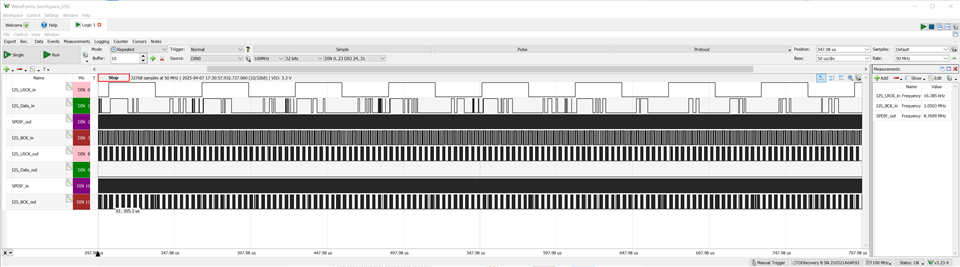
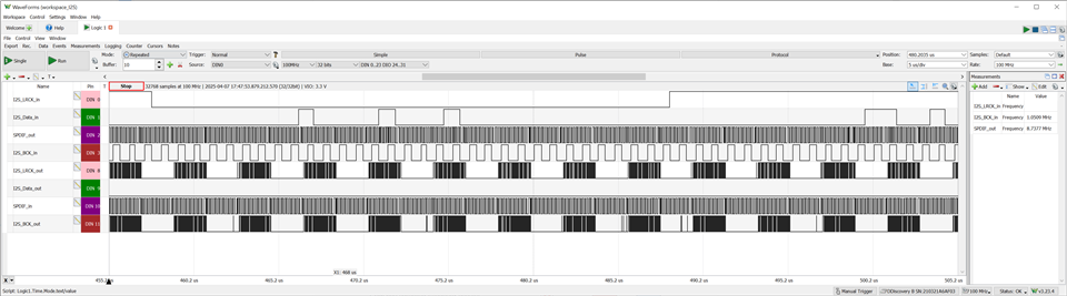
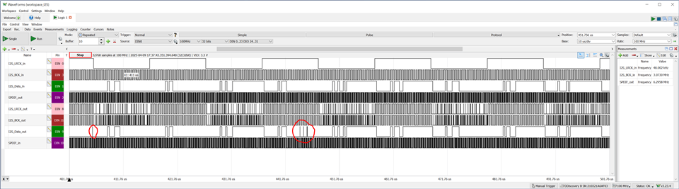
Not sure that parameters of input digital audio I2S are correct, but it seems that PCM9211 fails to convert it to S/PDIF: 0V ... instead of audiostream.

Here is my setup:

1. I2S parameters (configigured at the device that provides I2S):

  • LRCLK frequency: 48kHz
  • BCLK frequency: 48 x LRCLK frequency (i.e. 2.304 MHz)
  • word size: 18 bits

2. I2S is applied to the MPIO_C port of PCM9211:

  • BCLK --> MPIO_C1
  • LRCLK --> MPIO_C2
  • DATA --> MPIO_C3

3. PCM9211 is configured as follows:

  • Reg 0x6F: 0x05 ... enables DIT Standalone Mode
  • Reg 0x24: 0x14 ... set master clock XMCKO as XTI/2, i.e. 12.288 MHz; Enable Output
  • Reg 0x78: 0xCD ... route DIT Output (TXOUT) to MPO0 and XMCKO to MPO1

What is wrong with my setup ?

Thanks in advance

Pavel.

  • Hello Pavel,

    Each of the modules in the PCM9211 (DIR, DIT, ADC, Aux I/Os) only supports these four interface formats:

    • 24-bit I2S format

    • 24-bits Left-Justified format

    • 24-bit Right-Justified format

    • 16-bit Right-Justified format

    Also as a rule, the BCK has to fulfil the following equation,  otherwise even with supported bit length still it will not work:

    BCK= #of channels  x Bit depth  x Fs  

    PCM9211  in its default configuration will be able to do  I2S to SPDIF conversion.

    This question  (I2S to S/PDIF)  was posted  previously and you can refer to it in this link.

    https://e2e.ti.com/support/audio-group/audio/f/audio-forum/624635/pcm9211-how-to-convert-i2s-input-to-optical-s-pdif-output

    Kind Regards,

    Arash

  • Hello Arash,

    Thank you for answer.

    Regarding your formula BCK = # of channels x Bit depth x Fs, it seems contradictory with table 7-10 in the datasheet, where BCK = 64xFs. Going back to your formula and assuming the number of channels = 2, we get a bit depth = 32. The device that provides digital audio (MAX98089) can't generate such bit depth. So, PCM9211 and MAX98089 are incompatible ?

    Sincerely,

    Pavel.

    P.S. Tried to use GUI mentionned in the thread from your link. Doesn't work on my PC:

  • Hi Pavel,

    According to datasheet 32-bit interfaces are supported for the paths from AUXIN0/1/2 to MainPort/AUXOUT( refer to section 7.3.8.4 )

    The 64xFs implies for a stereo device,  the bit depth is 32 for this configurations as you mentioned. You have to see what bit depths you can provide form your source -that is also acceptable to PCM9211- and adjust your clocks according to above equation.

    The GUI works fine on windows 10 ( I just tried it without any EVM attached and it works fine). I assume it would work on older Windows as well since this is an old GUI anyway but I was told it has issue with windows 11. So try on different windows if possible.  If you have Win10, please try to reinstall the GUI and give it another shot. The good thing about GUI is that once you run the script it highlights the path or you can modify the path on the GUI yourself  which  makes it much easier to see  what you are doing. 

    If you still can not run the GUI after a reinstall on WIN10, create  a new post with   CODEC CONTROL SOFTWARE GUI issue     in the title  so the  software team can take a look at it (do not put any part number in the title)

    Regards,

    Arash

  • Hi Arash,

    Here is how formatting digital audio looks like at MAX98089 output: I use parameters as it is shown on the diagram at the bottom. Although is is shown for 16 bits, for my case I configured it for 24bits.

    On PCB I measure LRCK frequency: 48kHz and BCLK frequency: 3.072 MHz. Also I see some activity at SDIN ... in the sense that it is not stuck at 0. These settings appear to correspond to I2S, 24 bits.

    But nothing at all at the output MPO0.

    Even if the data on SDIN is somehow wrong, we should still see something on MPO0, shouldn't we?

    Regarding the GUI, the name of the executable you are using is CodecControl.exe... just to be sure we are talking about the same tool ?

    If YES, for creating new project, you use File --> New EVM Simulation ... --> Unknown ?

    Sincerely,

    Pavel.

    P.S. My OS is Windows 10

  • Hi Pavel,

    Arash is travelling for the beginning of this week. Please expect a delay in response.

    Thanks for your patience,
    Jeff McPherson

  • Hi Pavel, 

    For correct I2S, the first data bit has to come at the FALLING edge of 1st BCK , with respect to the edge of FSYNC clk,  as shown below. Make sure you adhere to the correct data format.

    The CodeControl is the correct GUI  and for me ( I don't have the EVM but even without the EVM connected) when I open the GUI , it is in the list of the available devices, thus I can see the script and registers. This old GUI doesn't need installation so it might misbehave on different computers, if possible try different PCs.

    Here is a sample script   that  you can modify  based on your needs,  but first you have to make sure your data format is correct otherwise even  with a good script  you may not get any activity at the output.  

    #**************************************
    #this script is for SPDIF-->RXIN0-->DIR-->MainOutput, Record sound from SPDIF to PC through TAS1020
    
    #So
    #1, Chose RXIN0 to DIR
    #2, Active DIR
    #3, chose DIR output as Mainoutput's source.
    
    #Also HW modification
    #1, Flying to High Level(3.3V) to make sure U7's output is Hi-Z
    #or 2, TAS1020 output logic high on P1.2 I2S enable signal. 
    #**************************************
    
    
    #System RST Control
    #w 80 40 00
    w 80 40 33
    w 80 40 C0
    
    #XTI Source, Clock (SCK/BCK/LRCK) Frequency Setting
    # XTI CLK source 12.288 and BCK 3.072, LRCK 48k = XTI/512
    w 80 31 1A
    w 80 33 22
    w 80 20 00
    w 80 24 00
    #ADC clock source is chosen by REG42
    w 80 26 81
    
    #XTI Source, Secondary Bit/LR Clock (SBCK/SLRCK) Frequency Setting
    w 80 33 22
    
    
    #*********************************************************
    #-------------------------------Start DIR settings---------------------------------------
    #REG. 21h, DIR Receivable Incoming Biphase's Sampling Frequency Range Setting
    w 80 21 00
    
    #REG. 22h, DIR CLKSTP and VOUT delay
    w 80 22 01
    
    #REG. 23h, DIR OCS start up wait time and Process for Parity Error Detection and ERROR Release Wait Time Setting
    w 80 23 04
    
    # REG 27h DIR Acceptable fs Range Setting & Mask
    w 80 27 00
    
    # REG 2Fh, DIR Output Data Format, 24bit I2S mode
    w 80 2F 04
    
    # REG. 30h, DIR Recovered System Clock (SCK) Ratio Setting
    w 80 30 02
    
    #REG. 32h, DIR Source, Secondary Bit/LR Clock (SBCK/SLRCK) Frequency Setting
    w 80 32 22
    
    #REG 34h DIR Input Biphase Signal Source Select and RXIN01 Coaxial Amplifier
    #--PWR down amplifier, Select RXIN2
    #w 80 34 C2
    #--PWR up amplifier, select RXIN0
    w 80 34 00
    #--PWR up amplifier, select RXIN1
    #w 80 34 01
    
    #REG. 37h, Port Sampling Frequency Calculator Measurement Target Setting, Cal and DIR Fs
    w 80 37 00
    #REG 38h rd DIR Fs
    r 80 38 01
    #***********************************************************
    #------------------------------------ End DIR settings------------------------------------------
    
    
    #***********************************************************
    #---------------------------------Start  MainOutput Settings--------------------------------------
    #MainOutput
    #REG. 6Ah, Main Output & AUXOUT Port Control
    w 80 6A 00
    
    #REG. 6Bh, Main Output Port (SCKO/BCK/LRCK/DOUT) Source Setting
    w 80 6B 11
    
    #REG. 6Dh, MPIO_B & Main Output Port Hi-Z Control
    w 80 6D 00
    #***********************************************************
    #------------------------------------ End MainOutput settings------------------------------------------
    
    # read back all registers to ensure GUI integrity
    r 80 20 5E

    Regards,

    Arsah

  • Hi Arash,

    Thanks for feedback.

    Concerning checking of the correct I2S formatting, I didn't check yet.

    To do that I need to workaround my custom board to connect multiple scope probes to get LRCK, BCK, and DATA signals simultaneously. This isn't so simple, given the lack of space for solder probes.

    Anyway I advanced in my investigation. Still not sure if the I2S coming from the MAX98089 is correctly constructed, I managed to convert it to S/PDIF and get it on the MPO0 pin. For that I changed one line in my programming code.

    Code before (not working):

    #Configure PCM9211
    # 1. To enable DIT Standalone Mode, set Register 0x6F = 0x05
    DIT_Standalone_Mode_En = (0x6F, 0x05, "Enable DIT Standalone Mode, MPIO_C3 = TXDIN, MPIO_C1 = TXBCK, MPIO_C2 = TXLRCK")
    # 2. Set master clock XMCKO as XTI/2, i.e. 12.288 MHz, Enable Output
    Master_CLK_Freq = (0x24, 5<<2, "Set master clock to 12.288MHz")
    # 3. Enable S/PDIF on MPO0 and XMCKO on MPO1 (p. 111)
    MPO0_DITOUT = (0x78, 0x0D | 0x0C << 4, "Route DIT Output (TXOUT) to MPO0 and XMCKO to MPO1")
    # 4. Select RXIN0 as the S/PDIF Input (DIR)
    DIR_RXIN0 = (0x34, 0x00, "Select RXIN0 as input for DIR")
    # 5. Route DIR Output to Main Output Port (MOP)
    MOP_DIR = (0x6B, 0x01, "Route DIR Output to Main Output Port (MOP)")
    
    Config_PCM9211 = (DIT_Standalone_Mode_En, Master_CLK_Freq, MPO0_DITOUT, DIR_RXIN0, MOP_DIR)
    I2C_ADDR = I2C_ADDR_PCM9211
    print("Programming PCM9211 ...")
    for reg_addr, reg_value, comment in Config_PCM9211:
        data = (c_ubyte*2)(reg_addr, reg_value)
        dwf.FDwfDigitalI2cWrite(hdwf, c_int(I2C_ADDR<<1), data, c_int(2), byref(iNak))
        if iNak.value != 0:
            print("Device power NAK "+str(iNak.value))
            quit()
        else:
            print(comment)

    Working code:

    #Configure PCM9211
    # 1. DIT Function System Clock Source <-- AUTO; DIT Bit clock, LR Clock, Data Source <-- AUXIN1
    DIT_Function_Control = (0x60, 0x04, "DIT Function System Clock Source <-- AUTO; DIT Bit clock, LR Clock, Data Source <-- AUXIN1")
    # 2. Set master clock XMCKO as XTI/2, i.e. 12.288 MHz, Enable Output
    Master_CLK_Freq = (0x24, 5<<2, "Set master clock to 12.288MHz")
    # 3. Enable S/PDIF on MPO0 and XMCKO on MPO1 (p. 111)
    MPO0_DITOUT = (0x78, 0x0D | 0x0C << 4, "Route DIT Output (TXOUT) to MPO0 and XMCKO to MPO1")
    # 4. Select RXIN0 as the S/PDIF Input (DIR)
    DIR_RXIN0 = (0x34, 0x00, "Select RXIN0 as input for DIR")
    # 5. Route DIR Output to Main Output Port (MOP)
    MOP_DIR = (0x6B, 0x01, "Route DIR Output to Main Output Port (MOP)")
    
    Config_PCM9211 = (DIT_Function_Control, Master_CLK_Freq, MPO0_DITOUT, DIR_RXIN0, MOP_DIR)
    I2C_ADDR = I2C_ADDR_PCM9211
    print("Programming PCM9211 ...")
    for reg_addr, reg_value, comment in Config_PCM9211:
        data = (c_ubyte*2)(reg_addr, reg_value)
        dwf.FDwfDigitalI2cWrite(hdwf, c_int(I2C_ADDR<<1), data, c_int(2), byref(iNak))
        if iNak.value != 0:
            print("Device power NAK "+str(iNak.value))
            quit()
        else:
            print(comment)
    

    Both are extracts from my Python scripts I use to program my board over I2C using Digital Discovery.

    As you can see only 1st comand changed. I don't remember why I chose this "DIT Standalone Mode" option to be able to input digital audio from the MPIO_C port - maybe ChatGPT advised me to do so. Anyway it doesn't work. For the 2nd version (the one that works), I was inspired by the example "PC Record via TAS1020 through MPIOC in DIT output.txt" that I found in the CodeControl folder. In this version input of DIT module is selected to be AUXIN1 and by default AUXIN1 is function of MPIO_C port.

    Nevertheless there are still problems. When I provide optical loopback (i.e. MPIO0 output --> optical transceiver --> optical cable --> RXIN0) and measure BCK, LRCK at Main Output Port, they differ from BCK, LRCK rpovided by MAX98089 (that are applied at MPIO_C). Also, nothing on DOUT, although there is activity on DIN.

    Here are differncies:

    BCK_in frequency: 3.074 MHz;  BCK_out frequency: 477.13 kHz

    LRCK_in frequency: 48 kHz;      LRCK_out frequency: 7.45 kHz

    DATA_in: activity:                        DATA_out: nothing at all

    Can we draw some conclusions at this stage ... from my setup and the measurements made, or it is necessary to workaround PCB in order to test several signals at the same time?

    Regarding issue with CodeControl I could fix it: the problem is that the tool doesn't take into account regional settings.

    Changing "decimal symbol" from ',' to '.' fixes the issue.

    Sincerely,

    Pavel.

  • I just got back to office and will take a look at it as I go through my to do list.

    Regards,

    Arash

  • Hi Pavel,

    With this experiment I still suspect the conversion of formats has some issue .  I think the safest and fasted method is to send a proven correct I2S format along with the initial script; it should work right away and once you have a working set up ,you can do minor and major modifications. 

    Thanks for letting us know about the issue with the reginal format of decimal and comma.

    Regards,

    Arash

  • Hi Arash,

    Here are waveforms for digital audio configured at MAX98089 as I2S, 24 bit

    • I2S_LRCK_in: connected to MPIO_C2 (comes from MAX98089)
    • I2S_Data_in: connected to MPIO_C3 (comes from MAX98089)
    • I2S_BCK_in: connected to MPIO_C1 (comes from MAX98089)
    • SPDIF_out: connected to MPO0 (goes to optical transceiver, then into opt. cable)
    • I2S_LRCK_out: connected to LRCK of Main Output Port (goes to dedicated pin of MAX98089)
    • I2S_Data_out: connected to DOUT of Main Output Port (goes to dedicated pin of MAX98089)
    • I2S_BCK_out: connected to BCK of Main Output Port (goes to dedicated pin of MAX98089)
    • SPDIF_in: connected to RXIN0 (loopback from SPDIF_out over optical cable)

    Zoomed:

    What about correctness of I2S, generated by MAX98089 ?

    Sincerely,

    Pavel.

  • Hi Pavel,

    Looking at the the BCKO,  it doesn't look correct. 

    It is supposed to be a continues and periodic clk as seen in BCKI . With the  same token, the LRCLKO is also strange and doesn't look correct. ( Both look similar to each other here ).

    The BCKI and LRCLKI look okay to me ( of course still I  can not verify that DIN  of each I2S channel  is happening at the first falling edge of 1st BCK or not ).

     S/PDIF format is different and the  information is imbedded in the s/pdiff signal,  so I can not comment on it. The DIX9211 has a calculator which is  connected to the  output of the DIR and calculates the actual sampling frequency of the incoming S/PDIF signal. So you can imagine it is not something that one can check by looking at the plots.

    Sometimes when I am checking my format from an unknown/untested source, I   use a DAC and send the  I2S ( 1KHz sinewave)  to a  DAC and monitor the resulted analog sinewave. If you have a DAC handy, you can verify your format with it first and then test PCM9211 with the verified I2S format.

    Wit the  dedicated GUI, you also don't need to be worry about registers ,  as it will set them up for you according to your desired configuration. 

    Regards,

    Arash

  • Hi Arash,

    Here is captured video from Digital Discovery that shows how I2S in/out and S/PDIF in/out evolve when I apply at about 5 sec 1 kHz SIN to MAX98089 audio input. The duration of this SIN about 10 sec.

    Any comments ?

    Thanks

  • Hi Arash,

    Here is the suggestion I received from Gemini 2.5 Pro AI after reporting him the issue:

    Your input I2S data (I2S_Data_in) changes correctly when you apply the sine wave.

    The PCM9211's DIT block is NOT processing this changing input data.

    The SPDIF_out signal remains stuck outputting the same static pattern (representing incorrect/garbage payload data) regardless of whether the input is silence or a sine wave.

    The DIR correctly locks to the S/PDIF framing but decodes the same incorrect static payload data in both cases.

    The problem is squarely located in the DIT block failing to correctly sample or process the I2S_Data_in signal.

    Given all the previous steps, the overwhelming likelihood remains the incorrect I2S Bit Clock (BCK) frequency coming from the MAX98089. The DIT simply cannot reliably latch the input data bits when the clock timing is off (even if the DIR can lock to the resulting frame).

    Next Step:

    You must find a way to configure the MAX98089 to output the correct BCK frequency of 3.072 MHz (64 * 48 kHz). Consult the MAX98089 datasheet or configuration tool documentation to see how to achieve the standard 64xFs BCK ratio when it's operating as an I2S Master at 48 kHz. Until that input clock is corrected, the PCM9211 DIT is unlikely to function correctly.

    Ar you agree with such conclusion ?

    Sincerely,

    Pavel.

  • Yes, i agree,

    issue  from beginning  was with I2S. ( I thought your clks were correct and were according to the equation). Anyway,  I think the DAC method is a very simple method to make sure I2S is correct. but any type of verification should be ok.

    Regards,

    Arsh

  • Hi Arash,

    Unfortunately, we were unable to obtain support from Analog Devices: all our attempts were in vain. In terms of support, TI is far superior compared to Analog Devices. So at the moment I don't know how to be sure to provide correct I2S to the PCM9211. But regardless of Analog Device, I continue to explore PCM9211. Here's the setup that leaves me a little perplexed and where MAX9808 has nothing to do with it.

    Configuring I2C...
    Programming PCM9211 ...
    0x40 <-- 0x33
    0x40 <-- 0xC0
    0x60 <-- 0x04
    0x61 <-- 0x13
    0x6F <-- 0x00
    0x24 <-- 0x14
    0x78 <-- 0xCD
    0x34 <-- 0x00
    0x6B <-- 0x04
    0x37 <-- 0x07

    In this code I redirect I2S signals (received on MPIO_C) to Main Output Port (register 0x6B). So I2S signals (LRCK, BCK, Data) are forced by this setup to be identical. But as you can see from oscillograms only Data (except for some glitches) are identical, but LRCK, BCK are completely different. How to explain this?

    Sincerely,

    Pavel.

  • Thanks Pavel,

    Yes, something looks fundamentally wrong with Fs and BCK out-- as not only they are not uniform ( or 50-50  pulses) , it seems LRCLK  is same as  BCK , not in the form of 32*LRCLK or 256*LRCK or 64*LRCLK  and etc. 

    If you are using the GUI, it writes the registers based on you desired/selected  configuration and that by itself should eliminate  any incorrect register issue.

    Another attempt might be to send a signal to ADC only , When the DIR is unlocked, the ADC output is automatically routed to the Main Output Port and you can see if you are getting the correct signal. ( if yes, you can send it back to PCM9211 as it is a correct I2S format ) 

    I was checking your code for register 6B  and you are using AUXIN1 ( so  with ADC as input set it to 0000000 ( default)  and check  the main output port. 

    You have to try different ideas/routs until you get it running and then you can go back to the original configuration of your choice. Since we suspect the input I2S has an issue, with ADC test you will be sending an analog signal instead. 

    Regards,

    Arsah