This thread has been locked.

If you have a related question, please click the "Ask a related question" button in the top right corner. The newly created question will be automatically linked to this question.

NE5532A: High failure rates with new die design

Part Number: NE5532A
Other Parts Discussed in Thread: NE5532

Tool/software:

Hi Raymond,

We are having failures on the production line in China using the new Malaysian parts.  We had not experienced any failures using the older Mexican parts with more than a years production.

These are operational failures, not performance failures.  The failure rate is a few percent.  I have not yet visited the factory, it is in China, to see the issue first hand.

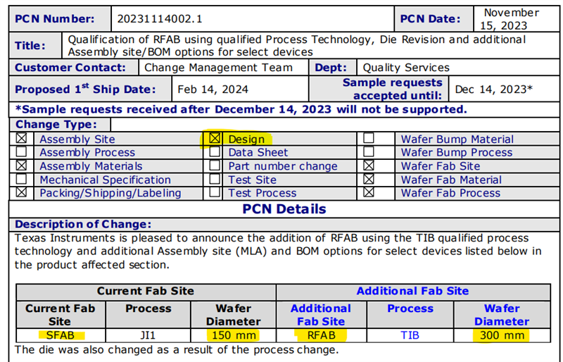
From posts on this forum it appears that you have redesigned the part in a new silicon process to fit a fab running larger wafers.  I'm afraid you have changed the device operation in the process.

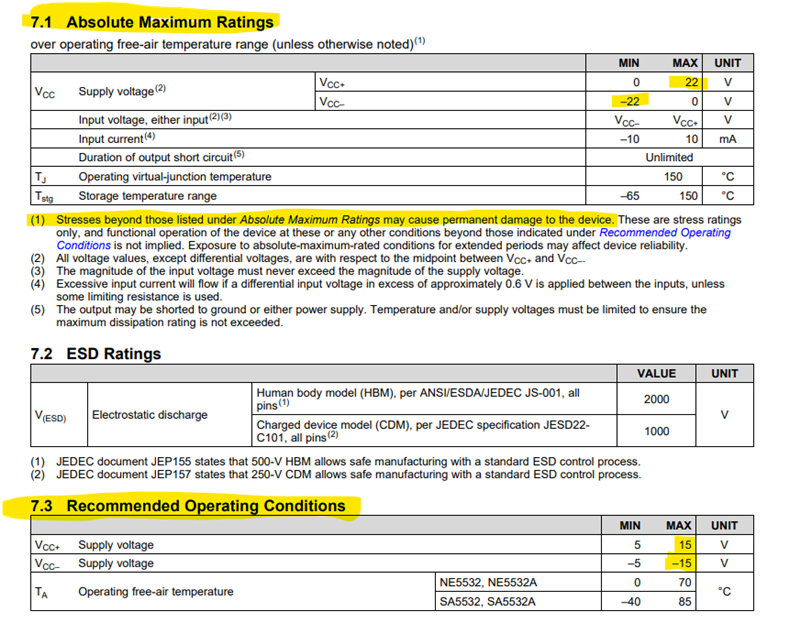
We are running the parts on +/-17V rails, which should not be a problem for the NE5532 since it is rated for +/-22V operation.  However, another post implies you aren't supporting anything above +/-15V.  The original 5532 from Signetics was designed for the higher voltages and this has been a hallmark of the 5532 ever since.

I cannot share schematics publicly but can send them through private message.

Rich

  • Hi Rich, 

    The PCN went out on November 15, 2023 and can be found here:

    https://mm.digikey.com/Volume0/opasdata/d220001/medias/docus/5726/PCN20231114002.1.pdf

    Below you can see that the device was redesigned and moving from the old SFAB 150 mm process to the new fab (RFAB) with the 300mm process. The product will no longer be available from the old fab site as SFAB is closing permanently. Until all material runs out it is possible upon ordering to receive either die. 

    The datasheet lists the Absolute max to be 22V and recommended at 15V. Stresses beyond the abs max can permanently damage the device. I am looking into if the abs max has changed. We don't specify parameters for anything beyond the +/-15V range. 

    Best Regards, 

    Chris Featherstone

  • I saw this notice already.  It doesn't explain the difference in the chip designs.

    I have since received more information about the problem on the production line.  They were driving all 16 inputs of the product with maximum level test signals (+24dBu) before powering the product up.  This presents the opamps with 34Vpp at their inputs with no voltage on their power supply pins.  

    The new chips are a new design, implemented on a different process, in a different fab. The older chip design may have had protection against this situation which was left off the new chip design. It could also be that the new process changed breakdown voltages at various places in the design and the new devices are therefore more sensitive to overvoltage when they have no supplies.

  • Hi Richard, 

    We can discuss further over private E2E messages. I will send a friend request via E2E. Based on your description it looks like the device inputs are subject to very high overvoltage events at the contract manufacturer and the old device seemed to still function or not degrade too severely under the overvoltage events. Let's sync up over the private E2E messaging. 

    Best Regards, 
    Chris Featherstone