This thread has been locked.

If you have a related question, please click the "Ask a related question" button in the top right corner. The newly created question will be automatically linked to this question.

OPA1679-Q1: OPA1679IRUMR thermal pad connection

Part Number: OPA1679-Q1
Other Parts Discussed in Thread: OPA1679,

Tool/software:

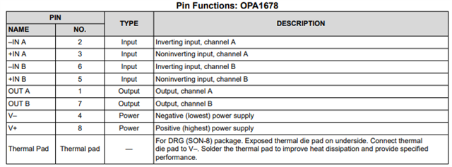
In a recently developed board I have connected the exposed pad to GND instead of V- (V+=+9V, V-=-9V) 

In the following post https://e2e.ti.com/support/audio-group/audio/f/audio-forum/1315924/opa1679-q1-about-thermal-pad/5007921?tisearch=e2e-quicksearch&keymatch=opa1679%20current I have read that, by connecting the exposed pad to any other voltage above (V-) may result in current leakage that increases at the elevated temperature.

And this is what I'm experiencing on the board: if I heat the IC, the current consumption rise up to many times the current consumption which is specified in the datasheet, and this is the leakage effect which is described in the post.

In order to try to save the first batch of PCBs here my question: is possible to keep the exposed pad elettrically isolated from the PCB pad with a thermal pad? The exposed pad will dissipate heat to the PCB but it will be elettrically floating.

Thanks in advance for your support

Best Regards

Jonata Ubbiali

  • Hi Jonata, 

    In OPA1679's datasheet, the the use of thermal pad is specified--> this is the recommended use. 

    is possible to keep the exposed pad elettrically isolated from the PCB pad with a thermal pad? The exposed pad will dissipate heat to the PCB but it will be elettrically floating.

    Electrically isolated means the the thermal pad is not connected to any signal. This is not a best practice. At least, you may tie the thermal pad to GND rather than allow it to potential to float for now (until the next revision). By connecting the thermal pad to GND, the IC's substrate is "seen" a known GND potential, which is better than floating the IC's Si substrate.

    If you have other questions, please let me know. 

    Best,

    Raymond

  • Hi Raimond,

    thank you very much for your reply. 

    Ok, therefore I have to modify the gerber because my current PCB configuration has the exposed pad connected to the GND instead of V-; the OPA1679 is used in an audio amplifier and when the board heats I have some audio issues (noise and pop). I have measured the current consumption on the -9V rail and it passes from about 80mA (expected value for 28 single opamps used in the circuit) up to 1A if I heat the IC to 80°C, which is very abnormal behavior. In this condition the IC temperature suddenly rises to above 200°C. 

    I would try to fix the configuration by disconnecting the exposed pad from the GND and connect it to the V- and see if the issue disappear.

    Best Regards

    Jonata Ubbiali 

  • Hi Jonata, 

    This does not seem to be that this is thermal pad connection or termination issue. 

    You mean that you have 28X of OPA1679-Q1 on a PCB. How are these op amps connected among each other? Are you parallel some of these to increase the output current. 

    If you are paralleling op amps, you need to take are the output stage as follows. 

    https://www.ti.com/lit/ab/sboa553a/sboa553a.pdf?ts=1753397640887&ref_url=https%253A%252F%252Fwww.google.com%252F

    Please let us know what you are trying to accomplish. Maybe the PCB is unable to dissipate the amount heat and you need to increase the heat dissipated area to disperse the heat. 

    Best,

    Raymond

  • Hi Raymond,

    thank you for the information provided.

    This is an audio amplifier with 4 balanced audio inputs; each input is preamplified by 1xOPA1679: two input buffers, one differential amplifier and one inverter. We have no opamp parallel connections. The only wrong thing I see here to justify this strange behavior is the exposed pad connection

    Thanks

    Best Regards

    Jonata

  • Hi Jonata,

    The only wrong thing I see here to justify this strange behavior is the exposed pad connection

    The thermal pad should be connected to Vee or -9Vdc in this case, which the op amp's substrate will be reverse biased.  If there is an excessive current flow per your description, the PN junction is likely forward biased when P-substrate is tied to GND (and N well layer is more negative than P substrate). 

    if I heat the IC, the current consumption rise up to many times the current consumption which is specified in the datasheet, and this is the leakage effect which is described in the post.

    The description is possible, since PN junction has typical -2mV/C in thermal coefficient. Higher IC temperature, less voltage is required to forward biased the PN junction interface. But I will make sure that the IC has not been damaged first. 

    If you tie the thermal pad to -9Vdc, does the excessive current condition disappeared when the op amp heats up? I the headphone connected to the differential output. 

    BTW, in your difference amplifier, you could use 10kΩ feedback resistors instead of 100kΩ, If you do, increase the feedback capacitors from 15pF to 150pF. 100kΩ will increase your audio's thermal noise unnecessarily. 

    When you convert single-ended to differential output voltage, you could use a reference voltage rather than GND. Yes, you have a resistor tied to non-inverting input, but a reference voltage will have better isolation effects (especially if GND is noisy), since your output is a differential output, see the application note below. 

    https://www.ti.com/lit/an/sbaa265a/sbaa265a.pdf?ts=1753689780348&ref_url=https%253A%252F%252Fwww.google.com%252F

    If you have other questions, please let me know. 

    Best,

    Raymond

  • Hy Raymond,

    thank you very much for your help and advice.

    Best Regards