This thread has been locked.

If you have a related question, please click the "Ask a related question" button in the top right corner. The newly created question will be automatically linked to this question.

TLV320AIC3268: Programming the mini-dsp's

Part Number: TLV320AIC3268
Other Parts Discussed in Thread: PUREPATHSTUDIO

Tool/software:

Just designed a system with the aic3268. This system requires to mux two 32bit mono pcm buses from ASI2 and ASI3 to a 8-channel TDM bus on ASI1. Also in opposite direction. So two channels from TDM on the Din on ASI1 to the DOUT of ASI2 and ASI3.

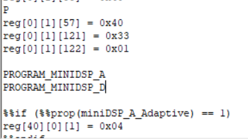
Found out that for this configuration I need to program one or both mini-dsp's. So in the meantime I have purepathstudio running and the aic3268 is listed under frameworks.

However I don't have an usb-i2c programmer with the TAS1020B or an evaluation board. And it seems like the evaluation board is obsolete.

So my question is: How am I be able to program the mini-dsp's on the aic3268?

I do have a EVAL-ADUSB2EBUZ available(also usb-i2c). Furthermore I noticed the TTK USBtoI2X dongle on: https://e2e.ti.com/support/audio-group/audio/f/audio-forum/299026/ttk-reference-designs-for-audio-converters

Can I order such a dongle anywhere? Could I design it myself? And I think the TAS1020B needs firmware for that, where could I find that?

Sorry for that much questions, but I would like to know if it's even possible what I am trying to accomplish.

  • Hi Robin,

    Many of our experts are out of office right now, so please allow until next week to receive a response.

    Best,

    Garret

  • Hi Robin,

    If you have a way to program I2C onto the chip, you can use PPS to generate some I2C code that you can then flash, no extra hardware needed. If you go to Build->Generate Code, it creates a file in the folder you saved the process flow to, called "base_main_Ratexx.cfg" where Ratexx is the sample rate that the flow compiled for. This is a regular .cfg file that we would use on some other software, like the PurePath Console, or CodecControl. The lines with "> xx" are shorthand for writing to the next register, as shown here:

    I am not familiar with that USB I2C board, but if you are able to connect to the SCL and SDA lines on the AIC3268, you should be able to program the miniDSP - the .cfg file that PPS generates contains the code to program the miniDSP sections of the device.

    Can you share your PPS diagram so far? I am confused where the ASI2 and ASI3 mux to ASI1 is - I do not think miniDSP or the device can transfer TDM slots between ASIs, but we can route signals from one ASI to another.

    Let me know if you need more help.

    Best,
    Mir

  • Hi Mir,
    Thank you for your response.

    Regarding the I2C, I'm going to give it a try with the converter. On the board there's already a mcu. So if it will not work with the converter I can always do it through the mcu. In the end it has to go that way anyway.

    I'm not new to your audio codecs, however I'm very new to your mini-dsp codecs. So I'm not sure if I use the right components.

    At the moment I still get the message:

    Generating code for base_main_Rate44 .. assembling ...MemoryType usage: miniDSP_A_coeff: 6, miniDSP_A_coeff0: 1, miniDSP_A_coeff1: 5, miniDSP_A_data: 28, miniDSP_A_instr: 57, miniDSP_A_instr_alloc: 57, miniDSP_A_cycles: 67, miniDSP_A_cycles_alloc: 67,miniDSP_D_coeff: 6, miniDSP_D_coeff0: 1, miniDSP_D_coeff1: 5, miniDSP_D_coeff2: 0, miniDSP_D_data: 12, miniDSP_D_instr: 84, miniDSP_D_instr_alloc: 84, miniDSP_D_cycles: 36, miniDSP_D_cycles_alloc: 36

    Assembly failed
    Error: aic_main.asm(-1): Could not arrange blocks, check addresses and try again

    Best regards,
    Robin

  • Hi Robin,

    I tried to recreate your process flow here, and I noticed that it did not fail when the "Multi_Channel_Dig.." were at 4 channels, but when I changed it to 6 or 8, it failed. This has to do with the estimated clock cycles for the miniDSP (such as IDAC/IADC) along with the default clock rates in the SystemSettingsCode commands. I was able to get it to compile correctly when I enabled "SynchMode" - this is an important setting that lets us pass data between the DAC and ADC and vice versa by powering them up at the same time and synchronizing their clocks. It is done through a series of register writes that are already in SystemSettingsCode by default. Let me know if you need more explanation here, but I hope this compiles and works as you expect!!

    Best,
    Mir

  • Hi Mir,

    Very nice. Thank you very much. Now I have the h-file with register values and the cfg-file. Do I understand correctly that the order of writes should be:

    1->system reg values

    2->minidsp A values

    3->minidsp D values

    I also see some pll register writes but not all of them, I think. Is there a way that the processflow will include all the clock settings too? Because I only configured the sample rate to be 48kHz. I never configured any clock input. On the pcb I have a 12Mhz clock to the mclk-pin.

    Are there any other important things in the processflow where I don't know about?

    And is this the right approach? Or do you think it's possible without the minidsp's?

    Again, thank you very much so far!

    Best regards,

    Robin

  • Hi Robin,

    I think this is the correct approach for this non-standard routing. I know it is difficult, but we will get it to work!

    The cfg file should have all the PLL settings from SystemSettingsCode, and if there are things left out, they will have been software-reset to the default values from the software reset command at the beginning of the script. And yes, the writes will follow this order, and then have more code at the end (as specified in systemsettingscode). The miniDSP A and D values are set in the "PROGRAM_MINIDSP_A" or D lines as shown, and then the code is generated in that place in the cfg file:

    The clock input will be whatever the default is. It is likely MCLK, if you send your systemsettingscode I can verify for you.

    Are you able to get the passthrough working as expected? It would be a few days for me to check in the lab, earliest I could do it would be next week. So let me know what your status is on getting this to work and I can help virtually here.

    Best,
    Mir

  • Hi Mir,

    Thank you very much.

    At the moment I'm using the .h-file that's created by PPS, because I don't yet have a tool that can read it in and use my I2C converter. I wrote a I2C function for the mcu that's writing the three arrays of structs.

    1. Writing REG_Section_program[ ]

    2. Writing miniDSP_A_reg_values[]

    3. Writing miniDSP_D_reg_values[ ]

    4. I try to do my own PLL and clock settings.

    5. Still have to do the correct ASI settings

    Step 4, I do because then I can just replace the .h-file that's newly created from PPS.

    Now I'm struggeling to get some confirmation that there's something happening in the codec. I tried to configure DOUT1 as CLKOUT to check the clock that's coming from the PLL. The register writes get acked. I can also read them back correctly. Also I tried to configure the DOUT1 as GPO and set it, that's working.

    Probably I missed something here, I'll keep trying.

    Best regards,

    Robin

  • Hi Mir,

    Dout1 with the clock from the PLL is working now. It seems to be the right clock. This was just for testing.

    Next step is configuring the asi's.

    Will let you know.

    Best regards,

    Robin

  • Hi Mir,

    At the moment I'm struggeling a bit to get the right clocks on the ASI's. The DAC clocktree seems to be configured correct. However the ADC clocktree is not. It seems that the mux between the NADC and the MADC dividers is stuck on taking the DAC_CLK. I tried to configure the clocks for a 12MHZ input clock and Fs of 48KHz as stated in attached table.

    Then I thought if it could something to do with the synchronise function in PPS. But when I comment out the writing of the PPS h-file, the ADC_CLK is still coming from the DAC_CLK.


    My question is: are the values of table 32 right in my situation? Also do I have to bother about the "To DAC miniDSP clock generation" and the "To ADC miniDSP clock generation" labels in figure 58 on page 66 of the datasheet? Because should they be synchronised or not, as per table 32?

    Looking forward to hear from you.

    Best regards,

    Robin

  • Hi Robin,

    First, why are you trying to set DAC and ADC clocks differently? For SynchMode to work, we need ADC and DAC clocks to be the same, so the miniDSP clocks are the same. You can see in the help file for the device in PPS:

    And by default, NADC is powered down in the SystemSettingsCode file. The clocks in that chart you posted should work, but make sure you follow these instructions on how to get the interprocessor working (aka SynchMode). You can see the default system settings code files for when each of these things get set, but I would recommend just changing the section that you need for the 48k option, like here:


    Best,
    Mir

  • Hi Mir,

    Thank you for your response.

    I did this because table 32 said so. However I didn't know.... So now I have the two clocks the same. Also have the right clocks on ASI1-3. Only still have not the right signals on the Din and Dout of the asi's.

    I now have:

    ASI1, BCLK = 12.288MHz, WCLK = 48KHz(8-chn@32-bit, DSP)

    ASI2, BCLK = 1.536MHz, WCLK = 48KHz(2-chn@16-bit I2S)

    ASI3, BCLK = 1.536MHz, WCLK = 48KHz(2-chn@16-bit I2S)


    Then tried to loopback through the dsp from ASI2 to ASI2, that didn't work yet. Now trying with a tonegenerator connected to all outputs to get something out of it. Till now no succes...

    I attached the .cfg and .h file with the tone generator connected to the outputs.

    6153.base_main_Rate48_pps_driver.h1777.base_main_Rate48.cfg

    After writing all values from the .h-file I'm writing values below for the PLL and the ASI's.

        //make sure to be in he correct book and page
    	tlv_write(0,0x00);		//jump to page 0
    	tlv_write(127,0x00);	//jump to boek 0
    	tlv_write(0,0x00);		//jump to page 0 van boek 0
    
    	//setting up clock
    	tlv_write(60,0x80); //power up miniDSPA & D together
    
    	tlv_write(4,0x33); //adc/dac clk
    	tlv_write(5,0x00); //clkin				MCLK & Low PLL
    	tlv_write(6,0x91); //PLLP & PLLR		1 & 1
    	tlv_write(7,0x07); //PLLJ				7
    	tlv_write(8,0x06); //PLLD				1680
    	tlv_write(9,0x90); //PLLD
    	tlv_write(10,0x01); //PLL_CLKIN_DIV		1
    //	tlv_write(11,0x82); //NDAC				2
    
    	tlv_write(12,0x82); //MDAC				2
    	tlv_write(13,0x00); //DOSR				128
    	tlv_write(14,0x80); //DOSR
    
    	tlv_write(18,0x01); //NADC				power down
    //	tlv_write(18,0x87); //NADC				7
    //	tempval = tlv_read(18);
    
    	tlv_write(19,0x82); //MADC				2
    	tlv_write(20,0x80); //AOSR				128
    
    	tlv_write(11,0x87); //NDAC				7 and powerup at the end
    
    	//setting up ASI's
    	//ASI1
    	tlv_write(0,0x04);	//page4
    
    	tlv_write(1,0x38); 	//asi1 audio format			DSP/32bit/Dout not high imp
    	tlv_write(2,0x00);	//asi1 left chn offset
    	tlv_write(3,0x00); 	//asi1 right chn offset
    	tlv_write(4,0x26); 	//asi1 chn setup			DAC&ADC left & right chns
    	tlv_write(5,0x00); 	//asi1 adc bus format		Use R1 settings
    	tlv_write(6,0x00); 	//asi1 multipin				Data in & out single pins
    	tlv_write(7,0x01); 	//asi1 adc input ctrl		minidsp ADC data fed to ASI1
    	tlv_write(8,0x50); 	//asi1 dac data path		left-left right-right
    	tlv_write(9,0x00); 	//asi1 adc chn tristate		nothing tristated
    //	tlv_write(9,0xFF); 	//asi1 adc chn tristate		everything tri-stated
    	tlv_write(10,0x24); //asi1 clock outputs		bclk & wclk output
    	tlv_write(11,0x02); //asi1 bit clock			adc clk 12.28MHz
    	tlv_write(12,0x81); //asi1 bit clk n-div		1
    	tlv_write(13,0x00); //asi1 word clk n-div		-
    
    	tlv_write(14,0x01); //asi1 bclk & wclk output	bclk->div outp, wclk->adc_fs clk
    //	tlv_write(15,0xA0); //asi1 dout1				from asi1
    	tlv_write(15,0x00); //asi1 dout1				from asi1
    	tlv_write(16,0x00); //asi1 bclk & wclk			adc same as dac
    
    	//ASI2
    //	tlv_write(17,0x18); //asi2 format ctrl			i2s, 32bit, not Hi-Z
    	tlv_write(17,0x00); //asi2 format ctrl			i2s, 16bit, not Hi-Z
    //	tlv_write(17,0x01); //asi2 format ctrl			i2s, 16bit, Hi-Z
    	tlv_write(18,0x00); //asi2 data offset			0 bclks
    	tlv_write(21,0x00); //asi2 adc format			sames as r17
    //	tlv_write(23,0x05); //asi2 format ctrl			asi2[1:2] = minidsp_a_dataoutput[3:4]
    	tlv_write(23,0x01); //asi2 adc input ctrl		disabled
    	tlv_write(24,0x50); //asi2 dac output ctrl		left - dac data left, right - dac data right
    //	tlv_write(24,0x00); //asi2 dac output ctrl
    	tlv_write(26,0x24); //asi2 wrd/bit ctrl			bclk and wclk as output
    	tlv_write(27,0x02); //asi2 bdiv input			ADC_CLK
    //	tlv_write(28,0x84); //asi2 bclk div				powered up, 4
    	tlv_write(28,0x88); //asi2 bclk div				powered up, 8
    //	tlv_write(29,0xC0); //asi2 wclk div				powered up, 64
    	tlv_write(29,0xA0); //asi2 wclk div				powered up, 32
    	tlv_write(30,0x24); //asi2 bclk, wclk output	bclk - div outp, wclk - div outp
    	tlv_write(31,0x00); //asi2 dout					DOUT2 from ASI2
    //	tlv_write(31,0x02); //asi2 dout					DOUT2 from ASI2
    	tlv_write(32,0x00); //asi2 adc w/bclk			wclk - same as dac wclk, bclk - same as dac bclk
    
    	//ASI3
    	//also testing with 16-bit I2S
    
    	//tlv_write(33,0x18); //asi3 format ctrl		i2s, 32bit, not Hi-Z
    	tlv_write(33,0x00); //asi3 format ctrl			i2s, 16bit, not Hi-Z
    //	tlv_write(33,0x01); //asi3 format ctrl			i2s, 16bit,Dout Hi-Z
    
    	tlv_write(34,0x00); //asi3 data offset			0 bclks
    	tlv_write(39,0x06); //asi3 ADC inp ctrl			asi3[1:2] = minidsp_a_dataoutput[5:6]
    //	tlv_write(39,0x00); //asi3 ADC inp ctrl			asi3[1:2] = Z
    	tlv_write(40,0x50); //asi3 dac output ctrl		left - dac data left, right - dac data right
    	tlv_write(42,0x00); //asi3 wrd/bit clk ctrl		bclk default polarity, b/wclk power down when codec power down
    	tlv_write(43,0x02); //asi3 bdiv input			ADC_CLK
    //	tlv_write(44,0x84); //asi3 bclk div				powered up, 4
    	tlv_write(44,0x88); //asi3 bclk div				powered up, 8
    //	tlv_write(45,0xC0); //asi3 wclk div				powered up, 64
    	tlv_write(45,0xA0); //asi3 wclk div				powered up, 32
    	tlv_write(46,0x46); //asi3 bclk, wclk output	bclk - div outp, wclk - div outp
    	tlv_write(47,0x00); //asi3 dout					DOUT3 from ASI3
    	tempval = tlv_read(47);
    
    	tlv_write(55,0x21); //asi3 GPIO1/2				GPIO1 - ASI3_BCLK, GPIO2 - ASI3_WCLK
    	tlv_write(56,0x03); //asi3 GPIO3				GPIO3 - ASI3_DIN
    	tlv_write(86,0x54); //asi3 GPIO1				GPIO1 - ASI3_BCLK
    	tlv_write(87,0x50); //asi3 GPIO2				GPIO1 - ASI3_WCLK
    	tlv_write(88,0x74); //asi3 GPIO3				GPIO3 - ASI3_DIN
    	tlv_write(89,0x74); //asi3 GPIO4				GPIO4 - ASI3_DOUT
    

    Probably I'm still missing something here. Also don't know if I can use the tonegenerator like so. I changed the status in pps to "run", is that allowed?

    Best regards,

    Robin

  • Hi Mir,

    Just to get something working, I made the processflow below. It routes the audio from ASI2 to ASI3 and from ASI3 to ASI2. To ASI2 and ASI3, there's a bluetooth module connected. Both are paired with headphones. At the moment audio from ASI2 to ASI3 is working. However the GPIO3-pin, configured as Din for ASI3 seems to outputting data on the scope. Therefore there's no data from ASI3 to ASi2.

    3276.base_main_Rate48.cfg7080.base_main_Rate48_pps_driver.h

    Below are the settings that I do after loading the data from the .h-file.

        //make sure to be in he correct book and page
    	tlv_write(0,0x00);		//jump to page 0
    	tlv_write(127,0x00);	//jump to boek 0
    	tlv_write(0,0x00);		//jump to page 0 van boek 0
    
    	//setting up clock
    	tlv_write(60,0x80); //power up miniDSPA & D together
    
    	tlv_write(4,0x33); //adc/dac clk
    	tlv_write(5,0x00); //clkin				MCLK & Low PLL
    	tlv_write(6,0x91); //PLLP & PLLR		1 & 1
    	tlv_write(7,0x07); //PLLJ				7
    	tlv_write(8,0x06); //PLLD				1680
    	tlv_write(9,0x90); //PLLD
    	tlv_write(10,0x01); //PLL_CLKIN_DIV		1
    //	tlv_write(11,0x82); //NDAC				2
    
    	tlv_write(12,0x82); //MDAC				2
    	tlv_write(13,0x00); //DOSR				128
    	tlv_write(14,0x80); //DOSR
    
    	tlv_write(18,0x01); //NADC				power down
    //	tlv_write(18,0x87); //NADC				7
    //	tempval = tlv_read(18);
    
    	tlv_write(19,0x82); //MADC				2
    	tlv_write(20,0x80); //AOSR				128
    
    	tlv_write(11,0x87); //NDAC				7 and powerup at the end
    
    	//setting up ASI's
    	//ASI1
    	tlv_write(0,0x04);	//page4
    
    	tlv_write(1,0x38); 	//asi1 audio format			DSP/32bit/Dout not high imp
    	tlv_write(2,0x00);	//asi1 left chn offset
    	tlv_write(3,0x00); 	//asi1 right chn offset
    	tlv_write(4,0x26); 	//asi1 chn setup			DAC&ADC left & right chns
    	tlv_write(5,0x00); 	//asi1 adc bus format		Use R1 settings
    	tlv_write(6,0x00); 	//asi1 multipin				Data in & out single pins
    	tlv_write(7,0x01); 	//asi1 adc input ctrl		minidsp ADC data fed to ASI1
    	tlv_write(8,0x50); 	//asi1 dac data path		left-left right-right
    	tlv_write(9,0x00); 	//asi1 adc chn tristate		nothing tristated
    //	tlv_write(9,0xFF); 	//asi1 adc chn tristate		everything tri-stated
    	tlv_write(10,0x24); //asi1 clock outputs		bclk & wclk output
    	tlv_write(11,0x02); //asi1 bit clock			adc clk 12.28MHz
    	tlv_write(12,0x81); //asi1 bit clk n-div		1
    	tlv_write(13,0x00); //asi1 word clk n-div		-
    
    	tlv_write(14,0x01); //asi1 bclk & wclk output	bclk->div outp, wclk->adc_fs clk
    //	tlv_write(15,0xA0); //asi1 dout1				from asi1
    	tlv_write(15,0x00); //asi1 dout1				from asi1
    	tlv_write(16,0x00); //asi1 bclk & wclk			adc same as dac
    
    	//ASI2
    //	tlv_write(17,0x18); //asi2 format ctrl			i2s, 32bit, not Hi-Z
    	tlv_write(17,0x00); //asi2 format ctrl			i2s, 16bit, not Hi-Z
    //	tlv_write(17,0x01); //asi2 format ctrl			i2s, 16bit, Hi-Z
    	tlv_write(18,0x00); //asi2 data offset			0 bclks
    	tlv_write(21,0x00); //asi2 adc format			sames as r17
    	tlv_write(23,0x05); //asi2 format ctrl			asi2[1:2] = minidsp_a_dataoutput[3:4]
    //	tlv_write(23,0x01); //asi2 adc input ctrl		disabled
    //	tlv_write(23,0x03); //asi2 adc input ctrl		asi2[1:2] = asi2[1:2]
    	tlv_write(24,0x50); //asi2 dac output ctrl		left - dac data left, right - dac data right
    //	tlv_write(24,0x00); //asi2 dac output ctrl
    	tlv_write(26,0x24); //asi2 wrd/bit ctrl			bclk and wclk as output
    	tlv_write(27,0x02); //asi2 bdiv input			ADC_CLK
    //	tlv_write(28,0x84); //asi2 bclk div				powered up, 4
    	tlv_write(28,0x88); //asi2 bclk div				powered up, 8
    //	tlv_write(29,0xC0); //asi2 wclk div				powered up, 64
    	tlv_write(29,0xA0); //asi2 wclk div				powered up, 32
    	tlv_write(30,0x24); //asi2 bclk, wclk output	bclk - div outp, wclk - div outp
    	tlv_write(31,0x00); //asi2 dout					DOUT2 from ASI2
    //	tlv_write(31,0x02); //asi2 dout					DOUT2 from ASI2
    	tlv_write(32,0x00); //asi2 adc w/bclk			wclk - same as dac wclk, bclk - same as dac bclk
    
    	//ASI3
    	//also testing with 16-bit I2S
    
    	//tlv_write(33,0x18); //asi3 format ctrl		i2s, 32bit, not Hi-Z
    	tlv_write(33,0x00); //asi3 format ctrl			i2s, 16bit, not Hi-Z
    //	tlv_write(33,0x01); //asi3 format ctrl			i2s, 16bit,Dout Hi-Z
    
    	tlv_write(34,0x00); //asi3 data offset			0 bclks
    	tlv_write(39,0x06); //asi3 ADC inp ctrl			asi3[1:2] = minidsp_a_dataoutput[5:6]
    //	tlv_write(39,0x00); //asi3 ADC inp ctrl			asi3[1:2] = Z
    	tlv_write(40,0x50); //asi3 dac output ctrl		left - dac data left, right - dac data right
    	tlv_write(42,0x00); //asi3 wrd/bit clk ctrl		bclk default polarity, b/wclk power down when codec power down
    	tlv_write(43,0x02); //asi3 bdiv input			ADC_CLK
    //	tlv_write(44,0x84); //asi3 bclk div				powered up, 4
    	tlv_write(44,0x88); //asi3 bclk div				powered up, 8
    //	tlv_write(45,0xC0); //asi3 wclk div				powered up, 64
    	tlv_write(45,0xA0); //asi3 wclk div				powered up, 32
    	tlv_write(46,0x46); //asi3 bclk, wclk output	bclk - div outp, wclk - div outp
    	tlv_write(47,0x00); //asi3 dout					DOUT3 from ASI3
    //	tempval = tlv_read(47);
    
    	tlv_write(55,0x21); //asi3 GPIO1/2				GPIO1 - ASI3_BCLK, GPIO2 - ASI3_WCLK
    	tlv_write(56,0x03); //asi3 GPIO3				GPIO3 - ASI3_DIN
    	tlv_write(86,0x54); //asi3 GPIO1				GPIO1 - ASI3_BCLK
    	tlv_write(87,0x50); //asi3 GPIO2				GPIO1 - ASI3_WCLK
    	tlv_write(88,0x74); //asi3 GPIO3				GPIO3 - ASI3_DIN
    	tlv_write(89,0x74); //asi3 GPIO4				GPIO4 - ASI3_DOUT

    As mentioned, I configured GPIO3 as Din for ASI3. GPIO1, GPIO2 and GPIO4 seems to be correctly configured. Are there functions for GPIO3 that are overruling this functionality?

    Best regards,

    Robin

  • Hi Robin,

    I found something interesting in the datasheet - register 88 in page 4, which is the GPIO3 configuration register, does not explicitly mention it being used as ASI3 DIN, instead it is set in register 56: 

    So, setting register 88 to 0x74 is under the "reserved do not use" section. I see it says to set this earlier, in Table 51:

    I wonder if you set register 88 pin control to 00001, (register 88 to 0x04), even though it says it can be used for Data input for ASI1, maybe this is a typo and it is data input for ASI3 - GPIO3 should not be able to be DIN for ASI1, according to table 47 in the datasheet. Setting this register to be an INPUT will probably help. Let me know if it works! 

    Best,
    Mir

  • Hi Mir,

    Thank you very much. This indeed did the trick.

    When I first read this, I thought it was a bit strange. Because according to table 51 you have to set bits in a reserved piece of register. However, after that I didn't think about it much.

    So again, many thanks.

    Next step: configuring the ASI1 with TDM.

    Best regards,

    Robin 

  • Dear Mir,

    I'm trying to output some data from one of the I2S busses to ASI1 bus. Both ASI2 and ASI3 are 16-bit stereo @ 48KHz. ASI1 is 32-bit 8-channel TDM at 48KHz. How do I control in which channel the data is put? I tried different connections on the "Multi_Channel_Digital_Out_1", however the data seems to be always in channel one with no offset from the wclk-pulse. 

    Could you also confirm that the input off all asi's are seperate, however the output data channels are shared in "miniDSP_A_DataOutput[1:8]" ? Is it possible that the data that I have to output on ASI2 and ASI3 is not put in some of the channels of ASI1?

    Best regards,

    Robin

  • Hi Robin,

    First, have you verified that the clocks you need for this are outputting/input correctly? If this is happening as you expect, you will need a BCLK of 16*2*48k = 1.536MHz for ASI2 and 3, and BCLK of 32*8*48k = 12.288MHz for ASI1. Then the ASI1 data would have repeated samples for each I2S2 data point. I am not sure if the GUI will allow it, since the clocks are different.

    If you can verify that you are able to generate the correct clocks out, I would then say to run the miniDSP ASI1 as if it was at the same rate as the ASI2 and 3, and then the data will fulfil the 2x oversampling automatically. Then, you can configure ASI1 data offset with page 4 register 2, to place the samples in the correct channels. This is IF you are outputting the clocks, and if you are only looking to put the ASI1 data on consecutive channels. If you could explain how your clocks are working that would help me understand. Also, can you attach your SystemSettingsCode code and your .pfw file, rather than the .h and .cfg? It is more human-readable.

    Best,
    Mir

  • Hi Mir,

    What I'm trying to accomplish is to connect two bluetooth-modules with their own audio bus to a tdm-bus in both directions. The tdm-bus configuration is fixed because it's part of an already deployed system.

    The tdm-bus configuration is a 8-channel 32-bit tdm bus with a sample rate of 48kHz for both the input and the output bus.The two channels that need to be put to ASI2 and ASI3 are in channel slot 1 and 2 respectively in the output bus. Subsequently the audio from ASI2 and ASI3 have to be put on the output tdm-bus in channel slot 1 and 2. The other channels on this bus should be untouched.

    The two databuses connected to ASI2 and ASI3 from the module's are configurable per module. It's fine if they are mono. The options for these busses are:

    -I2S, 48kHz, 16-bit

    -PCM, 48kHz, 16-bit

    -PCM, 48kHz, 32-bit

    Progress till now is:

    All the clocks are set correctly, checked this with the scope. I now configured ASI2 and ASI3 as I2S 16-bit. I succeeded to get audio in both directions on ASI2 and ASI3. The previous processflow connects the ASI2 and ASI3 and I had full-duplex communication between the connected headsets.

    So my main concerns are:

    1. Is it possible to output the two channels(mono audio from ASI2 and mono audio from ASI3) to two channels in the output tdm on ASI1 without touching the other channels on that bus? While there's also audio from the input tdm to ASI2 and ASI3?

    2. Is that also possible with two 16bit I2S buses, and take the left channel from each bus(mono)? Because the left and the right channel are from the same source, so it's mono anyway.

    3. When I would like to switch to PCM 32-bit on the buses ASI2 and ASI3, which component do I need in PPS for these interfaces?

    To me it seems that, if I have to output the audio from the tdm input bus to ASI2 and ASI3, this would be in the channels "miniDSP_A_DataOutput3:4" and in "miniDSP_A_DataOutput[5:6]". The audio from ASI2 and ASI3, would be in "miniDSP_A_DataOutput[1:8]". They have to appear in slots 1 and 2 on the tdm output bus. How do I prevent the data in channels 3,4,5,6 to be present on the tdm output bus? See figure 108 below.

    Sorry for that many questions, but I have to know. If we can't left the remaning channels untouched, I think this isn't possible?

    Best regards,

    Robin

  • Hi Robin,

    I think this *should* be possible. Can you attach your .pfw file you are using? I can try to test it on the EVM. Taking the left channel from each is simple, we just only connect the left side. Passing the data from one ASI to another simultaneously should be fine. The interprocessor object is passing separate streams of data from the miniDSP DAC to ADC. Like you noticed, the miniDSP A and D have up to 8 simultaneous streams possible. It separates them out into ASI1 -> CH1 and 2, ASI2 -> CH3 and 4, ASI3 -> CH5 and 6. Then we have two more possible as well. For an 8 channel system I think it assumes all 8 channels are on ASI1. But, you can route these any way you like. You may want to do it all with the multi channel object and then define which channels are being sent to ASI2 and 3 in the SystemSettingsCode with register 23 or 39 (page 4) as shown in the diagram. Switching to "PCM" does not make sense, PCM is a data type once it is in the computer. Related to the codec, it is I2S, which can then be saved as PCM on the computer. So, you likely mean I2S 32 bits on these ASIs, which should be fine and I would recommend it over having two separate bit depths on separate ASIs. Since there is only one miniDSP A and 1 D, there is only one set of miniDSP clocks, so any changing in bit depths will mean some truncating of the data. 

    Best,
    Mir

  • Hi Mir,

    Thank you for your response.

    For the I2S on ASI2 and ASI3 from the modules I can only choose 16-bit depth, no option 32-bit is available. Only in pcm-mode I can choose 32-bit. It's like described in section 8.3.9.2.4.5 of the datsheet of this codec. However the module's wclk is a long frame sync, it's high half of the bit-depth, like I2S, but only one channel is sent out.

    So now still on 16-bit I2S mode on ASi2 and ASI3.

    For testing purposes I changed the TDM on ASI1 to 16-bit and also changed the bclk to half what it should be. So now it's 6.14Mhz. What should correspond with the data on ASI2 and ASI3 inputs. However I still only see data appearing on the first channel on the scope.

    Also have some strange behaviour, that when I connect the datapoints I2S_In2_1 and I2S_In3_1, through the iDSP_D_A, to the Multi_Channel_Digi output block on channel 1 and 2. Then I still have audio from ASI3 to ASI2 and from ASI3 to ASI3, as I can hear in the connected headsets. While reg 23 and reg 39 are set to channel [3:4] and channel [5:6]. Strange right?

    Attached you will find the pfw-file. I zipped it because uploading here didn't work.

    tlv320aic3268_pfw.zip

    Best regards,

    Robin

  • Hi Robin,

    Have you not changed the SystemSettingsCode section of your PFW file? This is where you can set registers. First, I would recommend you look at the ASI2 and 3 IN or OUT settings, this is register 23-40 on page 4 in the SystemSettingsCode. Lines 105-108 here:

    I will attach the SystemSettingsCode configuration that I took from your pfw, I like to open it in a text editor and paste it in separately. I removed all the non-48k configurations so it is a bit shorter and easier to read. Another thing to note is the clock settings in the system settings code - if you are changing the clocks on your MCU that provides the clocks to the codec, you will need to change the registers for the PLL and dividers as well. 

    I am happy to help you edit this file with the correct clock settings and config, if you can make it clearer what you are using.

    Best,
    Mir

    ssc.cfg

  • Hi Mir,

    In the beginning I didn't know about the SystemSettingsCode, so the mcu was writing the data from "base_main_Rate48_pps_driver.h" and then I was writing the settings for the clocks and the asi ports.

    I now changed it, I moved clock and ASI reg settings from mcu to the SystemSettingsCode. So the only thing the mcu now does, is writing everything from "base_main_Rate48_pps_driver.h". Attached you will find the pfw-file.

    With this pfw-file, I still have the behaviour of audio from ASI3 to ASI3 and from ASI3 to ASI2 with the headsets connected. Clocks for the ASI's seems to be right. However I don't know which clockfreq the minidsp needs? Audio from ASI2 to tdm on ASI1 looks ok on the scope, however from ASI3 to tdm out on ASI1 there's a lot of data on multiple channels.

    tlv320aic3268.pfw.txt

    What I'm trying to accomplish is below with tdm on 8-channel@32-bit, wclk=48KHz, bclk=12,288MHz

    Best regards,

    Robin

  • Hi Robin,

    Today is a U.S. holiday. Please be patient as our team follows up with you tomorrow.

    Thank you!
    Jeff McPherson

  • Hi Robin,

    To set the bit rate for each ASI, please check these registers:

    - Page 4 register 1: I see that you have it set to DSP and 16 bits, you probably want to set to 32 bits.

    - Do we need time slot mode for ASI1? If not, change register 3 and register 8

    - Since ASI1 is 32 bits, ASI1 N div can be set to 1 instead of 2

    - Remove page 0 registers 8 and 9, no D needed in J.D (or change to 0x00)

    Let me know how this goes.

    Best,
    Mir

  • Hi Mir,

    1. ASI1 is indeed in 16-bit now. This is just for testing purposes. Because you said:

    "I would recommend it over having two separate bit depths on separate ASIs."

    I will change it, to what it should be....

    2. Yes we need TDM or timeslotmode. The data from asi2 input should be in timeslot 1 and the data from asi3 input should be in timeslot 2.

    3. Of course, this should also be set correct accordingly.

    4. Why the D is not needed? My input clock is 12.000MHz on the mclk pin.

    Best regards,

    Robin

  • Hi,

    I had thought you were using 12.288MHz on the MCLK, since you had said this earlier:

    But if the input is 12MHz then it should be fine. 

    Another thing to note that I think may help solve your problems is to look into register [0][4][4] -> this register has a typo in the datasheet where it is missing bits 7 and 6. If we look at AIC3263 for example, or search B0_P4_R4 in the DS, we see that bits 7 and 6 establish multi-channel mode, so we can select 8 channels. However, this register is already set at the end of the system settings code script by default, and I see you have left this in:

    This setting should automatically set the time slot, as seen in section 8.3.9.2.5.2 of the datasheet. So, you do not need time slots and should change register 3 and register 8. This might help your multiple channels of data problem.

    Let me know what you are able to find here. And, if you can include scope shots of the different ASIs data that will be helpful as well.

    Best,
    Mir

  • Hi Mir,

    Thank you for your response.

    In the meantime I tried to get something on ASI1. However no matter what I configure, it seems that it doens't make a difference.

    Below is a scope snapshot of looping back data from ASI2 to ASI2(reg23). 

    Whereas:

    D0 = ASI1_BCLK

    D1= ASI1_WCLK

    D2=ASI1_DOUT

    D4=ASI2_WCLK

    D5=ASI2_BCLK

    D6=ASI2_DOUT

    D7=ASI2_DIN

    Below you will find scope snapshot and pfw file of the processflow where ASI2 input is connected to the multichannel output channel 1.

    7418.tlv320aic3268.pfw.txt

    Could you check if it does, what it needs to do on your board?

    Also, what should I use for the "Secondary audio serial adc interface format selection" and the "Tertiary audio serial adc interface format selection" in [0][4][21] and [0][4][33]?

    Best regards,

    Robin

  • Hi Robin,

    Mir is out of office and will return to this thread later this week.

    Best,

    Garret

  • Hi Robin,

    I wanted to let you know, I have been working on this for a while today. I have multichannel mode working with 4 channels at 32 bits right now. I will attach my PFW file and system settings code (I edit it separately so it is more readable). Next steps will be fixing the clock timing in ASI2 and potentially 3 (I just checked ASI2, and the clocks are slightly off in timing than ASI1 so I needed to mess with the settings on the AP receiver to get the data correctly, but it is a higher dBFS than expected). We can also work on getting 16 bit data passing through correctly to get all 8 channels. I am using 12MHz MCLK in, and the device is generating 48kHz WCLK out. Let me know if this is not what you expect. I will attach my APx project file as well so you can test the same thing as me.

    5153.ssc.cfg

    7418.tlv320aic3268.pfwhttps://e2e.ti.com/cfs-file/__key/communityserver-discussions-components-files/6/multi_5F00_asi_5F00_measurement.approjx

    Best,
    Mir

  • Hi Mir,

    Thank you that you're willing to try.

    I hooked it up to another dsp and programmed your project in the 3268. I noticed that the asi2 bit - and wordclock come from asi1. Also configured the bus of the other dsp as 4 channel, 32-bit, 48kHz. Then let it generate a sinewave. However there was no data appearing on the output on asi1. On the scope I have wclk from asi1 and asi2 at 48KHz and the bclk from asi1 and 2 at 6.12MHz. However no data.

    I think there should be data, right? Are there some other things wrong?  Are there other conditions that have to be met while writing the data from the h-file to the codec?

    Again, thank you very much for figuring out.

    Best regards,

    Robin

  • Hi Robin,

    Are you sure you had input on ASI1? You are using default DOUT1 pin for ASI1 I assume? Can you show your clock signals on the same scope as the input? What pin is the sine wave connected to?

    And yes, that is how I programmed the ASI2 clocks, I have found that the other ASIs need clocks to transmit data even if it is internally generated or copied from other ASIs.

    -Mir