This thread has been locked.

If you have a related question, please click the "Ask a related question" button in the top right corner. The newly created question will be automatically linked to this question.

TLV320AIC3268: TLV320AIC3268 miniDSP configuration

Part Number: TLV320AIC3268
Other Parts Discussed in Thread: MSP430F5510, TAS5548, PCM9211

Hello,

I am developing an audio product using PCM9211, AIC3268, TAS5548 and MSP430F5510.

My plan is that the AIC3268 receives I2S data signal from the PCM9211 on ASI1_DIN port. The received data is next filtered by AIC3268's miniDSP. Filtered data will then be sent to AIC3268's ASI1_DOUT port and go to TAS5548.

According to the signal routing between ASIs and niniDSPs diagram (copied below) shown in Figure 108 in AIC3268's datasheet, the data input path for ASI1 (by default) is:

ASI1_DIN --> ASI1_DataInput[1:8] --> miniDSP_D_DataInput_1[1:8].

The data output path for ASI1 (by default) is:

miniDSP_A_DataOutput[1:8] --> ASI1_DataOutput[1:8] --> ASI1_DOUT.

I think I must follow the above data input/output flow if I want to use the miniDSP. But I don't see a connection from the miniDSP_D to the miniDSP_A in the diagram.

I'm new to the audio parts. So my questions are:

1) How does the data go (or get filtered) from the miniDSP_D_DataInput_1[1:8] to the miniDSP_A_DataOutput[1:8]?

3) What kind of miniDSP filter scheme do you recommend for my application?

3) And how to configure AIC3268 miniDSP to do so?

Best regards,

Kevin

  • Hi, Kevin,

    1. In order to send data from the miniDSP_A to miniDSP_D or vice versa, I would recommend to use a PurePath Studio block called Interprocessor block:

    Interprocessor.pdf

    This block is used in cases where processing is needed with both miniDSP_A and miniDSP_D. In that way, you may receive data with the miniDSP_D and send it to the miniDSP_A. You may add filters before or after the interprocessor block if they are needed.

    2. Regarding the recommended filter, I would recommend to use the biquad blocks of PurePath Studio. These blocks have an internal graphical user interface that can be used to configure them in an easy way. You may add up to 10 instances per block if you require more filtering capabilities.

    3. PurePath Stuido is a great tool that is useful to configure the miniDSP. It automatically configures the registers of the AIC3268. You may request it in the following link:

    Please let me know if you have further questions or comments.

    Best regards,
    Luis Fernando Rodríguez S.

  • Hi Luis,

    Thank you for your reply! I've just requested the PurePath Studio in the link you provided.
    Is this software free? Can you please let me know the status of my request?

    Regards,
    Kevin
  • Hi, Kevin,

    Effectively, this software is free for our users. Our Audio Software team will verify your request. You should receive an email once they grant you access to download PurePath Studio.

    Best regards,
    Luis Fernando Rodríguez S.
  • Hi Luis,

    Now since I've got the PPS software I'd like to ask you a few more questions regarding my design. Recall my design plan which is the following:

    The AIC3268 receives I2S data signal from the PCM9211 on ASI1_DIN port. The received data is next filtered by AIC3268's miniDSP. Filtered data will then be sent to AIC3268's ASI1_DOUT port and go to TAS5548.  So I think the signal flow in the AIC3268 should be: ASI1_DIN -> AS1_DataInput[1:8] -> miniDSP_D_DataInput_1[1:8] -----> miniDSP_A_DataOutput[1:8] -> ASI1_DataOutput[1:8] -> ASI1_DOUT.

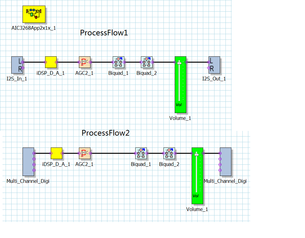
    According to my design, I created two process flows in PPS as shown below to configure miniDSP.

    Which one is correct? If they are incorrect, would you please create an example of PPS process flow to meet my design?

    Thanks,

    Kevin

  • Hi, Kevin,

    Could you provide the PPS process flows again? It seems that they didn't load correctly.

    Thank you.

    Best regards,
    Luis Fernando Rodríguez S.
  • Can you see the process flow picture now?

    Regards,

    Kevin

  • Hi, Kevin,

    Your first process flow (ProcessFlow1) is correct. Additionally, you may configure I2S_In_1 and I2S_Out_1 as one channel if you only require the left channel. Your second process flow is also correct, but we recommend to use the multi_channel input/output when more than 2 channels are required. So, please use your first process flow and let me know if you have additional questions or comments.

    Best regards,
    Luis Fernando Rodríguez S.
  • Thanks Luis!

    Questions:

    1) How to configure I2S_In_1 and I2S_Out_1 to one channel in PPS? I am unable to change the InputChannels or OutputChannels number in their Properties. Also, the I2S data comes in and goes out on a single port ASI1_DIN and ASI1_DOUT, why are there two channels Left or Right?

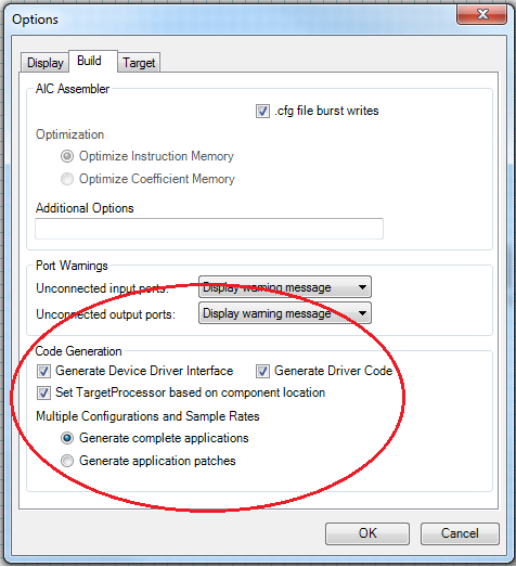
    2) Based on my first process flow, I generated the code using the following Build Options:

    The PPS automatically generated the following code/files:

         base_main_Rate44.cfg

         base_main_Rate44_pps_driver.h

         pps_driver.c

         pps_driver.h

    I don't have an interface (such as TAS1020B) on my application board to program the AIC3268 directly by the computer.

    The AIC3268 currently connects to a MSP430F5510 microcontroller via I2C. I'd like to program all register settings and coefficients into AIC3268 by MSP430 via I2C.

    I have a MSP430's source code - TIDA00609SW-1.0.1 which comes with my TI's PurePath Console Motherboard (PPCMB Rev.F, AIP006F).

    PPCMB uses AIC3262. A code/file in its firmware named "aic3262_1_code.h" seems to be very similar to the "base_main_Rate44_pps_driver.h" file generated by PPS for AIC3268 used on my board.

    So my question is: If I use the similar programming method as in the PPCMB firmware to program the AIC3268 on my board, can I simply replace the "aic3262_1_code.h" file with the "base_main_Rate44_pps_driver.h" file?

    Regards,

    Kevin

  • Hi, Kevin,

    1- The I2S_In and I2S_Out blocks can be configured as one channel by using another block. You may see in the InputOutput folder of PurePath Studio that there are two blocks called MonoI2S_In and MonoI2S_Out. These blocks are used when only left channel is required. Regarding your question about why are two channels, you may see in the AIC3268 block diagram that there are two ADCs and two DACs available. These channels refer to left ADC/DAC and right ADC/DAC. So, that's why there are two channels at the I2S blocks.

    2- Please take a look at this wiki article. It contains information about your question.

    e2e.ti.com/.../2823.how-to-generate-a-header-h-file-with-pps

    You may use the header file to configure the AIC3268 in an end system.

    Best regards,
    Luis Fernando Rodríguez S.
  • Hi Luis,

    I changed the InputOutput blocks to MonoI2S_In & MonoI2S_Out. How to configure AIC3268 in PPS to match my specific signal routing requirement for DATA, WCLK and BCLK signals?

    Here are the signal connections of my design: 

    AIC3268's Inputs: AIC3268's WCLK1 receives LR clock from PCM9211; AIC3268's BCLK1 receives bit clock from PCM9211; AIC3268's MCLK receives system clock from PCM9211; AIC3268's DIN1 receives data from PCM9211.

    AIC3268's Outputs: AIC3268's WCLK2 outputs WCLK to TAS5548; AIC3268's BCLK2 outputs BCLK to TAS5548; AIC3268's DOUT1 outputs data to TAS5548.

    Before using PPS I had to manually program specific registers to setup signal routing for DATA, WCLK and BCLK with the following code:

    // Book 0 / Page 4 / Register 11: ASI1, Bit Clock N Divider Input Control - 0x00 / 0x04 / 0x0B (B0_P4_R11)

     i2c8_write(AIC3268_ADDR, 0x0B, 0x04); // ASI1_BDIV_CLKIN = ASI1 Bit Clock Input Pin


    // Book 0 / Page 4 / Register 26: ASI2, Word Clock and Bit Clock Control Register - 0x00 / 0x04 / 0x1A (B0_P4_R26)

    i2c8_write(AIC3268_ADDR, 0x1A, 0x24); // 00100100: WCLK2 pin is output from ASI2, BCLK2 pin is output from ASI2 Bit Clock.


    // Book 0 / Page 4 / Register 27: ASI2, Bit Clock N Divider Input Control - 0x00 / 0x04 / 0x1B (B0_P4_R27)

    i2c8_write(AIC3268_ADDR, 0x1B, 0x04); // 00000100: ASI2_BDIV_CLKIN = ASI1 Bit Clock Input Pin


    // Book 0 / Page 4 / Register 30: ASI2, Bit Clock and Word Clock Output - 0x00 / 0x04 / 0x1E (B0_P4_R30)

     i2c8_write(AIC3268_ADDR, 0x1E, 0x13); // 00010011: ASI2_BCLK_OUT = ASI1 Bit Clock Input (ASI1_BCLK). ASI2_WCLK_OUT = ASI1 Word Clock Input (ASI1_WCLK).

    So again, how to create above code by PPS?

    Thanks,

    Kevin

  • Hi, Kevin,

    Your process flow is correct. However, if you are looking to use different clock sources (BCLK2, WCLK2, etc) you would require to modify the system settings code of the AIC3268 Framework. I recommend to take a look at the system settings code of the AIC3268 framework properties. You will see an entire code that is used as init code of the AIC3268. Then, you may add your code lines above to have these clocks correctly configured. You should get the correct clocks once you add these code lines and run the code.

    Please let me know if you have more questions or comments.

    Best regards,
    Luis Fernando Rodríguez S.
  • Hi Luis,
    Two questions:

    1) Where is the "system settings code of the AIC3268 Framework" located in PPS?
    Or did you mean that I need to go into the PPS generated header file to add my specific code there?

    2) I'd like to use both Left and Right Input & Output channels in PPS. But only one iDSP_D_A interprocessor with one link is allowed in the AIC3268 process flow. So how can I connect both L & R ports to iDSP_D_A component at the same time in process flow?

    Regards,
    Kevin
  • Hi Luis,

    I just noticed that I can change the InputChannels number to 2 in the properties of iDSP_D_A. So please ignore the second question in my previous post and reply on the first question. Thanks.

    Kevin
  • Hi, Kevin,

    I'm glad to read that you could increase the number of inputs in the iDSP_D_A block.

    Regarding your first question, you need to select the AIC3268App framework block. Once the block is selected, go to the properties window. There's a System Settings Code property that can be opened with a [...] button. You may access to the entire init file with this property.

    Best regards,
    Luis Fernando Rodríguez S.
  • Hi Luis,

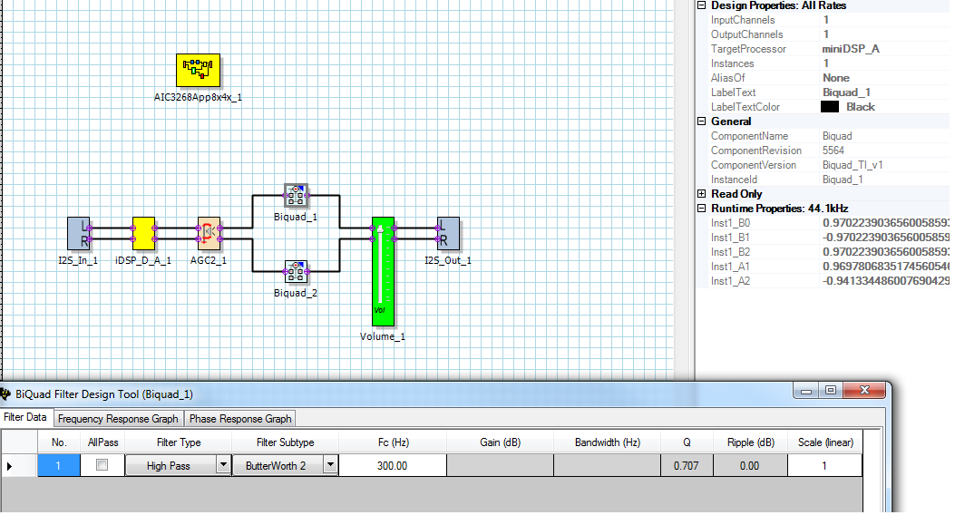
    1) Below picture shows my updated process flow with L & R channels. I also configured the Biquad_1 and Biquad_2 filter blocks to High Pass ButterWorth2 with Instance=1, Fc=300Hz. Do you think this setting is correct and a good starting point for the filter? Any suggestions to make a better audio filter? And any recommendations to improve my overall process flow (e.g. adding any components)?

    2) From learning PPCMB firmware, I noted that the system volume is controlled by Volume Coefficient using command line like this:

        aic3262_writeCram(aVolume[*pLevel], 1, AIC3262_MINIDSP_D, AIC3262_BUFFER_ADAPTIVE, 0);

    Is this how we should adjust the AIC3268 volume too?

    Can I simply reuse the aic3262.c and aic3262.h files that come with the PPCMB firmware to write AIC3268's CRAM?

    Or do I have to modify the following code listed in the aic3262.c file in order to use it for programming AIC3268?

    // AIC3262 C-RAM related information

    #define COEFFS_PER_PAGE 30

    #define BYTES_PER_COEFF 4

    #define CRAM_STARTING_REG 8

    #define CRAM_A_BOOK 40

    #define CRAM_A_BUFF_SW_PAGE 0

    #define CRAM_A_BUFF_A_PAGE 1

    #define CRAM_D_BOOK 80

    #define CRAM_D_BUFF_SW_PAGE 0

    #define CRAM_D_BUFF_A_PAGE 1

    #define BUFF_SWAP_TIMEOUT 10000

    Best regards,

    Kevin

  • Hi, Kevin,

    1) Your process flow filters seems to be all in order. Additionally, you may take a look at the frequency response graph to have more details about the filter that you configured.

    2) In this case, you can't reuse the .c and .h files of the AIC3262. The AIC3262 and AIC3268 have a different register map. So, you would require to make some modifications depending of your needs. However, the command that you mentioned could be used to modify the volume of the AIC3268.

    Best regards,
    Luis Fernando Rodríguez S.
  • Hi Luis,
    Thanks a lot for your help!!!

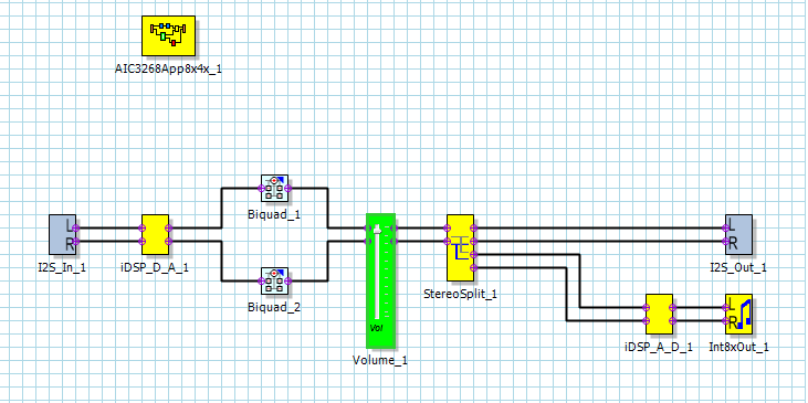
    How to add a headphone output in my process flow? I don't see a headphone output component in the InputOutput components folder in PPS.

    Regards,
    Kevin
  • Hi, Kevin,

    The analog outputs such line, headphone and speaker outputs are configured with the Int2xOut / Int4xOut / Int8xOut blocks for two channels and MonoInt2xOut / MonoInt4xOut / MonoInt8xOut for one channel.

    Best regards,
    Luis Fernando Rodríguez S.
  • Hi Luis,

    Based on my process flow, I was trying to adjust the AIC3268's volume by programming its B0_P0_R83 register for Left ADC Volume Control and the B0_P0_R84 register for Right ADC Volume Control. But it didn't work. What did I do wrong?

    Regards,
    Kevin
  • Hi, Kevin,

    I recommend several things:

    - In order to modify the ADC volume manually, you would need to eliminate the AGC2 block from your process flow. The AGC2 block modifies the PGA gain automatically. So, this could avoid a manual volume modification.
    - Then, you also may try with B0_P0_R59 and B0_P1_R60 to modify the PGA gain.

    Best regards,
    Luis Fernando Rodríguez S.
  • Hi Luis,

    I've deleted the AGC2 block from my process flow per your recommendation. But I still can't control the volume (Volume_1 block) by programming B0_P0_R83 register and B0_P0_R84 register. Below is my updated process flow:

    What did I miss? Do I have to program Volume_1 thru VolumeCoefficient? Any more suggestions on volume control? Thanks!

    Regards,

    Kevin

  • Hi, Kevin,

    Could you describe the procedure that you are using to modify the B0_P0_R83/84 registers? Are you modifying the registers while the process flow is running?

    Best regards,
    Luis Fernando Rodríguez S.
  • Hi Luis,

    My system is controlled by the MPS430 MCU, very similar to the PPCMB demo board. The firmware runs a state machine in where one of the states is used for volume control. So the MPS430 programs all registers including the B0_P0_R83/84 registers (PPS is not running/connecting the board, if that's what you meant)

    I know my volume control state is working because I have code (as shown below) in there to control the TAS5548's volume.
    //Adjusting TAS5548 volume
    aBuffer[0] = 0x00; // D<31:24>
    aBuffer[1] = 0x00; // D<23:16>
    aBuffer[2] = (Volume_tas5548[*pLevel] >> 8) & 0x00ff; // D<15:8>
    aBuffer[3] = Volume_tas5548[*pLevel] & 0x00ff; // D<7:0>
    i2c8_write_multi(TAS5548_ADDR, 0xD9, aBuffer, sizeof(aBuffer)/sizeof(uint8_t));

    Since I wanted to control the AIC3268's volume, I commented out above TAS5548 volume control code and added the following code to modify the B0_P0_R83/84 registers in aic3268.

    // Control AIC3268 ADC volume, 0 to 64 steps.
    i2c8_write(AIC3268_ADDR, 0x7F, 0x00); // Select Book 0
    i2c8_write(AIC3268_ADDR, 0x00, 0x00); // Select Page 0
    i2c8_write(AIC3268_ADDR, 0x53, Volume_aic3268_adc[*pLevel]); // Book 0 / Page 0 / Register 83: Left ADC Volume Control - 0x00 / 0x00 / 0x53 (B0_P0_R83)
    i2c8_write(AIC3268_ADDR, 0x54, Volume_aic3268_adc[*pLevel]); // Book 0 / Page 0 / Register 84: Right ADC Volume Control - 0x00 / 0x00 / 0x54 (B0_P0_R84)

    Volume_aic3268_adc[*pLevel] is a 65 size long array containing 8-bit value to be programmed into B0_P0_R83/84 registers. Every time the volume increase or decrease button pressed, the *pLevel will increase or decrease from 0 to 64 step (as same as for controlling the tas5548 volume).

    So above is my volume control procedure. Hope my description is clear to you.

    Regards,
    Kevin
  • Hi, Kevin,

    The Book 0 / Page 0 / Register 82-83 are used to modify the left and right ADC volume. If you refer to the DAC volume, the gain should be modified with other registers:

    Book 0 / Page 0 / Register 65: Primary DAC Left Volume Control Setting
    Book 0 / Page 0 / Register 66: Primary DAC Right Volume Control Setting

    Best regards,
    Luis Fernando Rodríguez S.
  • Hi Luis,

    Actually, I wanted to change the volume of the Volume_1 block (miniDSP_A) in my process flow. I noted that I could change the VolumeCoefficient of the Volume_1 block in PPS to control the volume. So I need a code to program VolumeCoefficient into aic3268's CRAM by MPS430 mcu. Do you already have such code that I may use? Thanks.

    Regards,
    Kevin
  • Hi, Kevin,

    You would need to verify the I2C address of the Volume Block that you are using. Please go to the properties window of the Volume Block in PPS. You will see a Component Interface section. This section describes which Book, Page and Register are being used to store the volume coefficient. In that way, you may modify the volume via I2C.

    Best regards,
    Luis Fernando Rodríguez S.
  • Hi Luis,

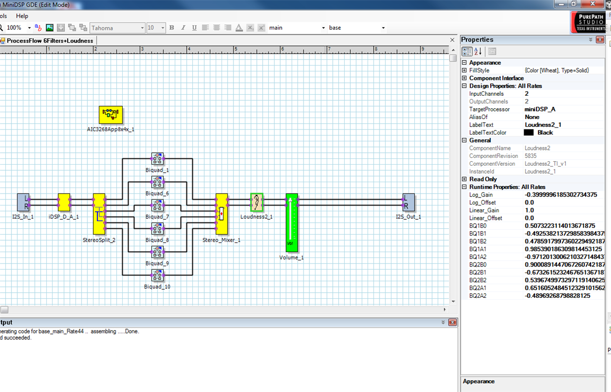
    I have a new question about the Loudness Filter block for aic3268 in the PPS. The image below shows my current process flow.

    Before I added the Loudness2_1 filter block into the process flow, my system was working fine and I could control the volume of my board by programming the Volume_1 block's VolumeCoefficient. After I placed the Loudness2_1 filter block into the process flow (as shown in above image), however, I was no longer be able to adjust the aic3268's volume and the volume of my board stuck at very high level (very loud).

    I used the default settings (such as Log_Gain, Log_Offset, Linear_Gain, Liner_Offset) listed in the Loudness2_1 properties as shown at right side of above image. Would you please advise how I should configure the Loudness filter correctly for my application?

    Thanks,

    Kevin

  • Hi, Kevin,

    The Loudness block basically works as a filter that modifies the volume depending of the frequency range. The frequency response curve corresponds approximately to the equal loudness curves of the ear. I recommend to take a look at the document below for the details about the Loudness filter:

    5684.Loudness.pdf

    Best regards,
    Luis Fernando Rodríguez S.

  • Hi Luis,

    May I ask you a new question? Below is my process flow for aic3268. What would be the simple method to increase the signal gain at my output?

    Best regards,

    Kevin

  • Hi, Kevin,

    You may use your volume block in order to increase the gain at the output. If you require additional gain, you may add another volume block.

    Best regards,
    Luis Fernando Rodríguez S.
  • Hi Luis,

    You mean to obtain additional gain I can add a second volume block after the first volume block like the following process flow?

    Regards,

    Kevin

  • Hi, Kevin,

    That's correct. In case you require more gain, you may add multiple volume blocks as you made in your last process flow.

    Best regards,
    Luis Fernando Rodríguez S.