This thread has been locked.

If you have a related question, please click the "Ask a related question" button in the top right corner. The newly created question will be automatically linked to this question.

TAS5162 chip breaks

Other Parts Discussed in Thread: PCM1808, TAS5086, TAS5162, DIR9001, TAS5162DKD6EVM, PLL1705

Hello!

a year ago I designed a class-D amplifier based on the TAS5162, pcm1808 and TAS5086. During the year, was made a few hundred samples intended to be sold to radio amateurs. Most devices are functioning properly and not cause any complaints from consumers. But some instances do not work properly.

Baseline data: Fpwm = 384kHz, PVDD = 38 V (stabilized), GVDD = VDD = 12 V, BTL mode, RL = 4Ohm, Roc = 22 kOhm. Circuit of the TAS5162
typical (as in Figure 15. Typical Non-Differential (1N) BTL Application With AD Modulation Filters).

The source of the signal typically used line-out computer sound card, headphone out of notebook.

Questions about the TAS5162:
in some cases, users complain about the failure of these chips in the long run the amplifier (more than 30min). First TAS5162 overheats and goes into protection mode, and then closes the power PVDD to GND, GND_x. Then comes the smoke and body chip breaks.
     
Rarely TAS5162 similarly fails at power on.

1. For whatever reason, may fail built-in protection TAS5162? Were there cases of unjustified failure of these chips in the past?
2. Is it possible failure of the chip, if heat sink is not grounded?
3. Does the quality of Low-Pass-Filter on the safety of the chip?

4. Why increase the supply voltage over 37V (Rl = 4Ohm - resistor) causes modulation of the output signal from the noise? This triggered a primary protection OCP?
 

Question about the TAS5086:
Sometimes there is a click when connecting / disconnecting the input from pcm1808. Then the sound just disappears. No reset or hardware enable / disable (pins PDN, RST) TAS5086 does not return it to normal operation. Only after the power cycling circuit begins to operate normally. The same problem sometimes happens in my other amplifier on the basis of TAS5504

schematic is here:

http://www.masterkit.ru/images/set_dop/bm2073_2.gif

http://www.masterkit.ru/main/scheme.php?num=1275

 I hope for your help, thank you!

  • Hello Evgeniy:

    I will be glad to assit you.

    1. The protection system works properly.

    2. The heatsink should definitely be grounded.

    3. The low pass filter is critical to the operation of the chip.

    4. As you mentioned, it appears that the primary OCP is tripping.  Does this occur when the device is cool or only when it is hot?

    Actions:

    1. Please send me the complete schematics of your system, I need to know what action it takes when OTW and SD are sent by the TAS5162.
    2. Please send me the GERBER files of your printed circuit board
    3. Please send me the IIC file that you use to set-up the TAS5086
    4. Please send me the specification (datasheet) for the inductors that you use in your output filter.

    TAS5086:

    I suggest that you change the resistors in your PLL filter from 220 ohms to 200 ohms.

    Can you read register x02 in the TAS5086?  It is the Error Register and will tell us if a clock error occurred.

    Regards,

    Fred

  • Fred Shipley said:
    4. As you mentioned, it appears that the primary OCP is tripping.  Does this occur when the device is cool or only when it is hot?

    Hi!

    It doesn’t depend on device temperature.


    1.         a) When OTW is sent by TAS5162, microcontroller U15 starts to reduce volume level in TAS5086 to prevent

    further overheating. And also the fan joins. It happens till OTW is active (low).

    b) When SD is set low by TAS5162, microcontroller U15 sets TAS5086 to PDN mode. If SD returns to normal state (high),  U15 restarts TAS5086 to operating conditions.


    2. GERBER files are in the attachments.


    3. Commands are sent via i2c to set-up TAS5086:

             a)  PIN PDN = 1

             b) Registers 0x1b =0x00,  0x05 =0x20,  0x19 =0x03,  0x10 = 0x03,   0x0e = 0b10110001

             c) hard un mute TAS5086 ( PIN MUTE=1)


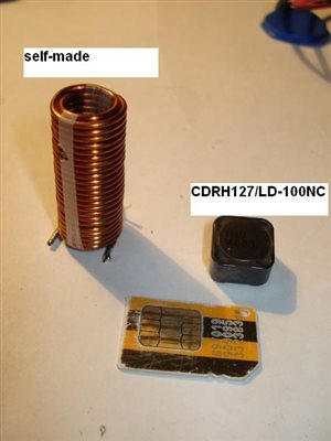
    4. I use  inductors CDRH127/LD-100NC.   Pdf is in the   attachments.


    5. I read register x02 in TAS5086 then it works well, data is 0x00.


    But In rare cases the sound disappears, and I hear a click in the speakers. This occurs from time to time

    in cases of connecting input signal to device or changing the input source between DIR9001 and PCM1808.

    Then I’m trying to read or write any data via i2c, but  TAS5086 does not  answer (registers read data is 0x00 or 0xFF) .  It’s seems, that it hangs...

    Only after RESET is pulled down and  TAS5086 is set up again,   it works normally.

    What is the reason of this problem, and how could I prevent it in the future?


    6. Last week I tried to course abnormal functioning of the device,  then TAS5162 goes to protection state or fails. Following your post «The low pass filter is critical to the operation of the chip» I used CDRH127/LD-100NC  in channel no.1, and self-made coil inductors in channel no.2 , so I could observe their influence .


    First I connect sine generator (0…5V, 1000Hz) to the input.

    PVDD set to +40V.

    speakers are disconnected

    «+» of the oscilloscope is connected to the positive out «SPKR_1CH_P», and its “-“ to the GND  


    Here what I found out:

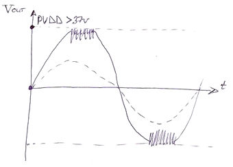
    During the increase of input signal level, the sine signal on the exit begins to be limited by supply voltage and gets a square form. BUT! At the certain moment it’s  modulated with  about 50kHz sine. It looks like autogeneration…  As we can see in the picture, the output voltage  accepts also the subzero values up to -20V.

    Under such circumstances   SD pin of TAS5162 goes low periodically and the device is stable.


    Then I increase PVDD up to +50V and repeat the experiment once again. Now, OCP repeats only 2-3 times and then… Clap… flashout…

    You can see consequences in the drawing:


    Device has failed.


                I understand, that CDRH127 is not  powerful enough for TAS5162 with load impedance 4Ohm (PVDD<=38,5). But how does the inductor influence  , if in tested circuit we have no load impedance?

    I read SLYT198 TI document (see attach.). There is posted, that “The designer who is primarily concerned with maximum heat and power-supply constraints and is not concerned with EMI and cuiescent current could use the Class-D amplifier without a filter to save cost”.  But actually it appears that the amplifier is very choosy to filter presence, and even more to its quality.

    May be it concerns only TAS5162? If it’s true, could you recommend any suitable commercial inductor for my device?


    6116.cdrh 127.pdf

    4135.schematic.pdf

    8424.slyt198.pdf


  • Hello Evgeniy:

    Thank you for sharing your Gerber files.  I am concerned that the grounding for the TAS5162 may contain too much parasitic inductance between the input ground and the output grounds.  Also, the decoupling capacitors for the PVDD pins should be placed no more than 2mm from their pins and 1mm is preferred.  If you update your PCB, please refer to the TAS5162DKD6EVM User's Guide (SLAU223) for PCB layout suggestions.  I would not advise routing PCB traces under the device, particularly in the top layer.

    I am working on getting a recommendation for an output inductor vendor;  however, a good "rule of thumb" is that the inductor should deliver at least 5uH of inductance at twice the overcurrent limit of the device.  The starting value is 10uH and its value can sag due to saturation and temperature effects.  In your case, with a 22K over current resistor, your over current limit should be ~12 Amps, so your inductor should be capable of at least 5uH of inductance at 24 Amps.  The paper you cited on output filters does not apply to a high power Class D power stage like this one.

    Class D amplifiers with LC output filters should not be tested without a load.  Without a load, the filter will begin to oscillate and cause an over voltage condition.  I understand that your oscilloscope traces were taken at the output of the filter; however, you will probably find similar waveforms at the output pins of the TAS5162.  The Absolute Maximum Voltage for this device is -0.3V to 71V and in your test, the voltage levels are outside the specification.  Please consult the datasheet for the Absolute Maximum Ratings for the TAS5162.

    If you experience an over temperature shutdown, you should wait a minimum of one second before you restart the TAS5162 to allow for some time to let the device and its heatsink cool.

    I will work on your TAS5086 question and report back to you.

    Regards,

    Fred

  • Hello Evgeniy:

    I am now looking at the clocking to the TAS5086.

    What is the purpose of the PLL1705?

    Have you taked a close look at your clocks going to the TAS5086 and do they conform to the criteria in the datasheet?

    What sample rate are you running?

    Can you put a crystal on the DIR9001 and let it run all of the time (at a 48kHz sample rate for example)?  It could then be used to clock both the PCM1808's (all of them in slave mode).  When it was locked and you wanted digital data, simply use the output of the DIR9001 for data to the TAS5086.  (You could then elimiate the tri state buffering for the audio clocks?)

    I am concerned about clock error.

    Regards,

    Fred