This thread has been locked.

If you have a related question, please click the "Ask a related question" button in the top right corner. The newly created question will be automatically linked to this question.

TPA3221: circuit destroyed

Part Number: TPA3221


Hi team,

I apologize for a late reply, but i didn't have opportunity to work with TPA3221. 

In the meantime I have created a smaller development variant where other modes can be set, but it is still not functional.

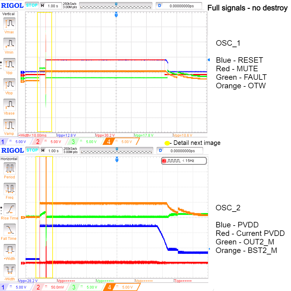
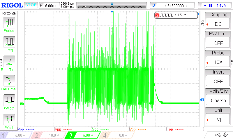
I send a two screenshot of oscilloscope.

At first is startup without destroy

(yellow-RESET,

light-blue - MUTE, 

pink- FAULT

dark-blue - OTW.)

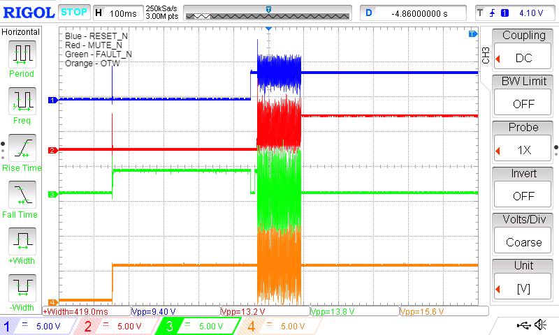
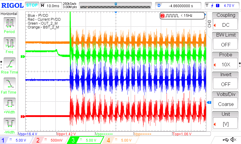
and second startup with destroy

(yellow-PVDD,

light-blue - RESET, 

pink- FAULT

dark-blue -VDD.)

-All input/output pin will were checkt -
-without output short circuit

PVDD = 12V
VDD = 5V (+-0.5)
I_pvdd = <0,1A
HEAD = 0
IN1_P = Nc
IN1_M = Nc
IN2_P = Nc
IN2_M = Nc
OUT_1_P = Nc
OUT_1_M = Nc
OUT_2_P = Nc
OUT_2_M = Nc

Does you have any idea ?
This is very important, because similar circuit doesn´t exist.

Thank you for your time

best regards 

Michael

  • Michael,

    What is the PVDD you are using. i am looking at waveform 2, seems like the voltage is just 12V? is that correct?

    Dylan

  • Hi,

    In the damaged power up waveform, it shows some glitch on the PVDD and then fault was pulled low. Have you checked what caused the glitches on the PVDD rail?

    Regards,

    Sam

  • Hi Dylan,

    Thank you for your reply.
    I use laboratory power supply 12V with 1A limit.
    Yes, it´s 12V ( minimal voltage of TPA3221 is 7V ).

    Michael

  • Hi Sam,

    Thank you for your reply.

    Input power terminals are goes on short-circuited (will cause destruction).

    Michael

  • Hi Michael,

    So the issue is relate to power short, right?

    Regards,

    Derek

  • Hi,
    yes, but on the output terminals isn't any short-circuit or any resistance (before destroy).  

    The output is unconnected.

    Michael

  • Hi Michael,

    Could you help to measure the pin shorts of PVDD/OUTx to GND?

    The damage you shows looks like a EOS damage, which only happens in high voltage/current situation. But checking the waveforms, there is no such situation and everything looks smooth(although the power rail/signals are still abnormal, like you have the PVDD glitches). 

    Can you make good supplies on PVDD/VDD/AVDD/GVDD, and then pull up the reset to see if the device will damage again? Let's just exclude the power supply impact.

    Thanks!

    Regards,

    Sam

  • Hi Sam,

    thank you for your reply. 

    Can i send you complet documentation (SCH, PCB,..) to your e-mail. 

    Before I destroy another circuit, I want to explore other options.

    Yes, the signals is abnormal, but PVDD is ok.

    I used laboratory power supply (HCS-3602 MANSON) 
    and there is nothing else between the PVDD and the power supply.

    Regards,

    Michael

  • Hi Michael,

    The schematic looks good.

    For the layout, PVDD decoupling MLCC caps should be placed on the same layer with the device, and be placed as close as possible to the PVDD/GND pins. This will have impact on the design robust level when outputting high power.

    But for your case, do you have any audio input when the damage happens? Looks like there is no output power, right? 

    The PVDD fluctuation happens right after the C_mute ramp up. I guess it's the moment when the device starts switching. I would recommend to capture the waveform to see the behavior of PVDD, OUTx pin(any of the PWM output), BSTx pin(the corelated BST to the OUTx). Trigger should be set as the negative edge of PVDD voltage(may be normal value -2V) to capture the moment of PVDD collapse.

    BTW, please also make sure there is no soldering issue which may also cause the damage...

    Regards,

    Sam 

  • An additional point is, the output inductor rating current is too low. The saturated current is recommended to be higher than the current limit of the device. 

  • Hi Sam,

    thanks for the comment, fix it in the next version.

    it wasn't connected any input signal or any output load.

    Before i destroy integrated circuit, i noticed a strange voltage peak. It´s a normal? In any case, the destruction occurred shortly after the supply voltage was connected. Can this destroy the integrated circuit?

    It's not bad soldering because I have already replaced 8 integrated circuits and I have 2 boards to test. In any case, the same defect.

    There is a bad coil in the scheme. but it has the same dimensions.

    Reagrds

    Michael

  • Hi Michael,

    It's not a normal behavior. The voltages had exceed the abx max range on datasheet. This may lead to damage. We need to find why there is such glitches rather than the PWM switching waveform in normal behavior.

    From the last waveform, I think the glitches show up when the device start to switching. Please zoom in the OUT_x waveform to see more detail. We need to figure out why it's not normal PWM waveform. In some cases, the insufficient power capability of the power supply could cause this kind of problem. Please check. 

    Thanks!

    Regards,

    Sam

  • Hi Sam,
    fortunately I saved the wave record. yes, I also think that before destruction, the circuit will start to switch.
     i will try to add capacitors closer to tpa3221 (including mlcc capacitors).

    Regards
    Michael
  • Hi Michael,

    The bulk PVDD cap is not so critical, but the MLCC should be place as close as possible to the pins.

    BTW, I would also suggest to have a zoom-in picture to check the PWM waveform when it start to switch. 

    Thanks!

    Regards,

    Sam

  • Hi Sam,
    Thank you for your answer.
    I added a 470u capacitor closer to the TPA3221 (including the MLCC 100n, 1u) and the result is the same. the difference is in the shape and length of the signal, but I don't know if it's significant.
    Regards
    Michael

  • Hi,

    The crosstalk among the channels is too high to identify much details from the waveform. The device is not damaged this time, it just didn't working well as expected, right?

    Looks like from some unknown reason, the CMUTE# pin is getting charged and discharged; and the abnormal behavior happens when the output ramps up to some level. Need to identify what happened at this moment. Please make sure the power supply has enough capability.

    You may remove the LC filter and measure the PWM output,(because the inductor in your design has limited rated current); capture the waveform on PWM output, at the moment the abnormal happens. The time scale should be in micro second range.

    Another point is, you are using head modulation in your design, coupled inductor may cause some issue here. If the PWM is normal without LC filter, could you change the inductor to non-coupling inductor?

    Regards,

    Sam

  • Hi Sam,

    Yes, the device was not destroyed, it just doesn't work properly.

    LC filter was removed and on the osciloscope i seen PWM output.

    Coil was added (to non-coupling SRP1265A-220M)- nothing change.

    Capacitor was added (output 1u) - nothing change

    connected sine signal - sine signal on the outputverything worked. After connecting to an 8 ohm load, about 45 W (1 channel, 30 V) was measured.

    The added capacitors hinded with the connection to the heatsink, so they were removed. the second time it was switched on, it was destroyed.

    during the month I will try to design a new circuit where I will use separate coils and add capacitors direct to the input of the integrated circuit. the peak that can be seen on the oscilloscope is likely to cause destruction. But i still don´t know, why the CMUTE# pin is getting charged and discharged.

    Is it possible that the paired coils caused the MUTE to charge and discharge? HEAD mode wasn´t active (connect to GND).

    Regards

    Michael

  • Hi Michael,

    CMUTE# pin can get charged and discharged when the RESET# is toggling. In the waveforms, glitches can be observed in multi signals. Is it fake glitches due to improper test setup, or it really exists? 

    If AD modulation is used, then the coupled inductor connected in your current schematic will actually take no effect. This is because the AD modulation always have a differential current flowing through OUTP and OUTN. The current flow into the coupled inductor from dotted and undotted terminal, neutralizing the magnetic field.

    Looks like when there is no LC filter, everything is good. Even non-coupled inductor is used, which means the device takes some current, the problem happens, right? Usually this kind of is related to the power supply and layout.

    If you are designing a new board, please follow the EVM layout design as much as possible to lower the risk... And make sure the power supply is stably working .

    Regards,

    Sam