This thread has been locked.

If you have a related question, please click the "Ask a related question" button in the top right corner. The newly created question will be automatically linked to this question.

CDCM6208-Output clock generation

Other Parts Discussed in Thread: CDCM6208, CDCM6208V1

Hello,

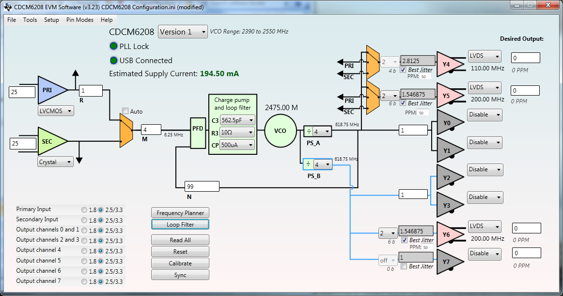
We are using CDCM6208 to generate below frequencies

1. 200MHz @ Y5

2. 200MHz @ Y6

3. 110MHz @ Y4

All are set as LVDS outputs. We feed 25MHz TCXO as the Primary Reference clock.

We have simulated for these frequencies in EVM software and we got the register values which are attached as text file with this post. With these values, in Simulation software, we are able to get accurate output frequencies. However when we load the registers on our custom board, the output frequencies are 116MHz @ Y4 and 208MHz @ Y5 & Y6.

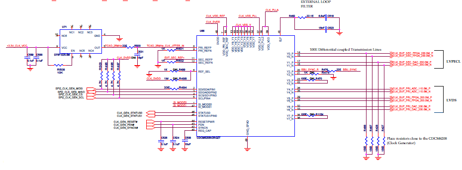
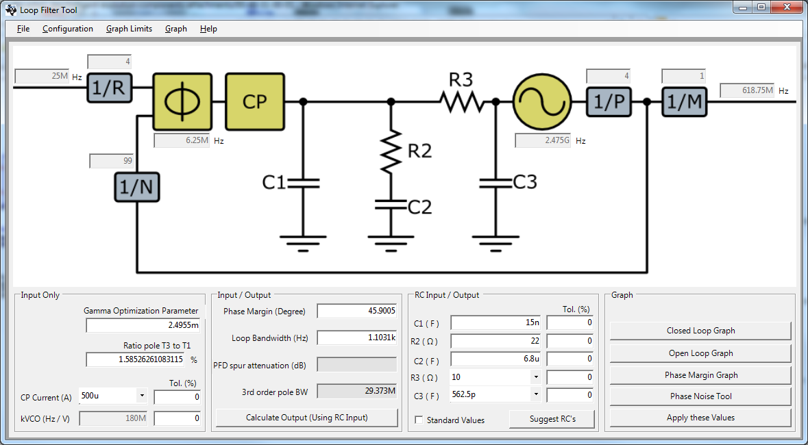
Why is this deviation? We have designed Loop Filter for 1KHz (The Schematics is attached with the post)

  • Hi Veerasamy,

    Please confirm that the images below represent the configuration you are trying to achieve.

    The configuration looks OK. I assume the TCXO input to PRI_REF is a clean 3.3V signal

    The CDCM6208 LVDS and LVPECL outputs need to be AC coupled (and in some cases DC biased externally) into the receiver. The output type is really CML when configured as LVPECL / LVDS. The 150 ohm resistors on Y0 and Y1 should not be populated when configured for LVPECL. These outputs (if used) would need to be AC coupled and DC biased externally.

    One reason why the outputs could be incorrect on power-up is failed PLL calibration due to premature toggling of the Power Down Pin (PDN) before the supplies to the device are stabilized. Also, the reference clock should be available and stable when the device powers up. Try re-calibrating the PLL by toggling the RESET pin after a faulty power-up. The TCXO input should be available and stable before a re-calibration is initiated.

    Regards

    Arvind Sridhar 


  • Hello Arvind,

    Yes the previous images are correct.

    We are loading CDCM6208, only after our FPGAs are configured on Board. So we have sufficient time for Voltage and reference clock to stabilize. Only after our FPGAs are configured, we are releasing the PDN pin high.

    We also tried to work with this logic, as represented in Flowchart in page 28 of datasheet.

    Powerdown pin -1

    wait;

    ResetN - 0;

    Wait;

    SPI WRITE;

    Wait;

    RESETN = 1;

    WAIT;

    SYNCN =1;

    We are making RESET to 0 before SPI writing. But with this setup, we are not getting Lock Detect signal.

    Only if we drive RESET pin high and then do SPI_Write, the register are properly loading and we are getting Lock Detect. This is contradicting statement on page 7 stating that RESETN can be held LOW while programming. Please clarify where the issue is? What is the WAIT period we need to give after RESET and PDN

    (We have made SI_MODE 1&0 as 00)

    Regards,

    Veerasamy

  • Hi Veerasamy,

    We are making RESET to 0 before SPI writing. But with this setup, we are not getting Lock Detect signal. Only if we drive RESET pin high and then do SPI_Write, the register are properly loading and we are getting Lock Detect

    So if I understand correctly, you are unable to get the PLL to lock when you program the device via SPI with RESETN=0 and subsequently drive RESETN=1 but get the PLL to lock correctly when programming with RESETN=1 from the very begining.

    In the condition where the PLL is not locked does toggling Register 3, bit 4 -> ENCAL result in a successful lock?

    Are you testing at room temperature?

    Just to confirm -> You are evaluating CDCM6208V1 and not CDCM6208V2

    Regards

    Arvind Sridhar


  • Hi Veerasamy, when you release the RESET pin to high state after programming the device while holding RESET pin low, then after releasing can you toggle register 3 bit 4 (ENCAL bit)? If it is already a "1", write "0" and then a "1". If you do this, does the PLL lock and lock indicator go high?

  • Hello Madhu/Arvind.

    We were able to solve the issue yesterday. We were using version 2, but we were programming for version 1. With Version 2 we were able to program properly and get correct output frequencies. I should have replied our progress to you earlier. Sorry for the delay.

    Thanks for the help.

  • Hello all,

    I'm facing the same issue on CDCM6208V2: after configuring the device to output 10 MHz from the secondary 25 MHz input clock (in I2C mode), even though it outputs the 10 MHz clock, I still don't have a valid Lock bit in R3.

    Is there a way to know when VCO calibration ended?

    Regards,

    Mihaita

  • The outputs are muted until the PLL is locked. Also you need to read R21 whether PLL is locked or not.

  • Hello,

    OK, but what I've noticed and is the same as  experienced, is that if the VCO calibration isn't done correctly then the PLL can lock with a wrong output clock. For instance if I configure the registers to output a 10 MHz clock and wait 100 ms for the VCO to calibrate and then assert SYNCN, the PLL will lock with an output frequency of 9.12 MHz. If I wait for 800 ms for the VCO to calibrate then the output frequency is 9.9991 MHz. So is there a way to know how much to wait on VCO calibration?

    Regards,

    Mihaita