Other Parts Discussed in Thread: LMC555, NE555, LM555, NA555, TLC551, SE555, TLC552, TLC555, SA555, CD74HC4060, SN74LV8154
This FAQ covers mono-stable circuits using the LM555, NA555, NE555, SA555, and SE555 timers that are called LM, NA, NE, SA, and SE individually hereafter. As a group they are call bipolar timers due to their design. This FAQ also covers LMC555 and TLC555 timers that are called LMC and TLC individually hereafter. As a group they are call CMOS timers due to their design. The FAQ is also applicable to the xx556, TLC551, and TLC552 timers.
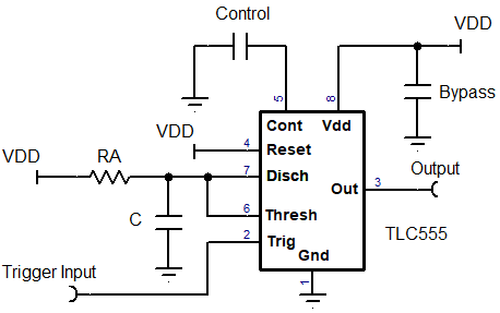
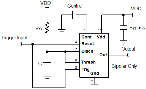
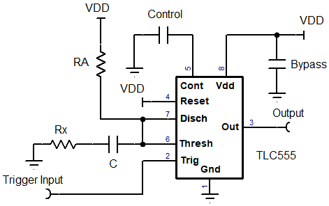
Mono-stable mode, as the name implies, has only one stable state. The stable state is output low. A trigger input voltage less than 1/3 of supply voltage starts a fixed width high output pulse whose length is based on an external resistor and capacitor value. The time required for capacitor voltage to reach peak value of 2/3 of the supply voltage is RA * C * Ln (3) = 1.1 * RA * C. This voltage will end the output pulse. The output will go back low and stay low indefinitely. The discharge pin also goes low and quickly discharges the capacitor back to zero. The trigger input should go high, > 1/3 supply voltage, before end of the output pulse because the trigger input is level sensitive, not edge sensitive.
If the trigger doesn’t return high before the end of the pulse, the output will be extended until trigger goes high. LM timer gives priority to threshold over trigger so the timer retriggers itself to start new cycles, which may result in a double width output pulse. Regardless of the timer used, it is highly recommended that the trigger returns high well before the end of the timing pulse.
Minimum time
The trigger pulse width must be wide enough to ensure the trigger input time is met. The LMC data sheet states 20ns minimum is sufficient and the other data sheets do not provide a minimum value. Reasonable minimums are proposed in the table. For trigger input low voltage that is not close to ground, double the table’s minimum trigger times. The minimum recommended time between trigger high and the end of timing pulse is based on the storage delay for the trigger comparator. All the data sheets had a recommend value of 10µs, however, the faster CMOS versions have neither long storage time nor a storage time that is a function of trigger low input voltage. Latest TLC commercial data sheet has been updated to 1µs to reflect this.
|
Recommended minimums |
LMC |
TLC |
LM |
NA,NE,SA |
SE |
|
Minimum input trigger width |
50ns |
100ns |
1µs |
1µs |
1µs |
|
Minimum trigger high to end of pulse time |
500ns |
700ns |
10µs |
10µs |
10µs |
|
Minimum output pulse width |
1µs |
1µs |
11µs |
11µs |
11µs |
Maximum time
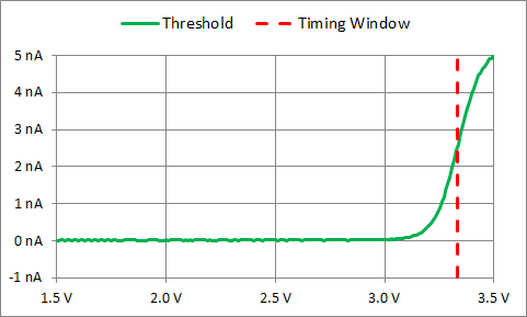
The maximum pulse time achievable is based on leakages in the capacitor, leakage and bias current in the timer’s threshold and discharge pins, and leakage on the printed circuit board. The circuit board can be the biggest source of leakage if contaminants or condensation is present. Leakage can also affect the accuracy of the time width because leakage changes the capacitor charging current. The threshold pin in the bipolar timers will start to draw a bias current near the threshold voltage. Therefore the bias current does not affect the charging current until the end of the timing pulse. The charging resistor current needs to be greater than the threshold pin current. The CMOS timers do not have a bias current. Due to the large capacitance needed for long pulse time, a nano-timer can be used as an alternative. They only require a single resistor to set the time delay up to 2 hours and use very little power. For even longer time up to 22 hours, CD74HC4060 has an internal oscillator that runs down to 0.1Hz followed by a 14 stage ripple counter. For almost any longer time including hundreds of years, consider 555 astable coupled to SN74LV8154 32 bit counter.
Typical Bipolar Threshold pin input bias current vs. threshold pin voltage. Supply = 5V
Accuracy
The actual length of the pulse will be slightly longer than the formula due to the propagation delay of the threshold comparator. This delay is not a significant factor unless the desired pulse length is close to the minimum time in the tables. In most cases, the tolerance of the timing capacitor will be the largest source of timing variance. Ceramic timing capacitors should be C0G/NPO type for the best temperature coefficient, voltage modulation, and aging characteristics. The timing resistor’s tolerance and temperature coefficient is also important.
The initial mono-stable timing accuracies are typically 1% on most of the data sheets. SE has a 1.5% maximum at 25C. The NE, NA, SA timers has a 3% maximum at 25C. The 1ms to 1.2ms limits in the LMC data sheet equate to 9.1% tolerance error which far too pessimistic. The LM and TLC have no maximum limits. The data sheets have no full temperature range limits for mono stable mode. For full temperature range final accuracy better than 4%, the cost of improving the timing capacitor and resistor may be higher than using a crystal oscillator plus logic counter solution.
Trigger Storage delay
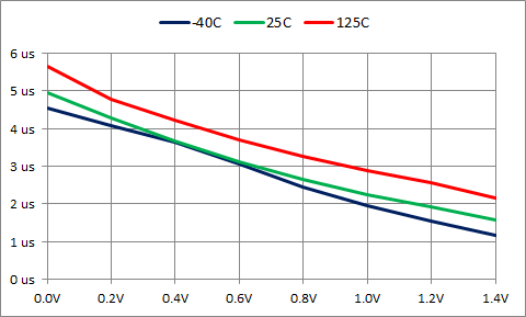
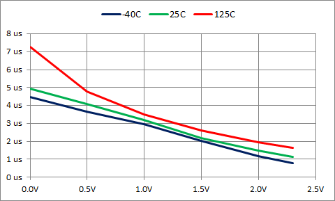
The storage delay of the trigger comparator varies with the previous trigger low voltage for the bipolar timers. The CMOS timer delays are not based on trigger low voltage. Typical TLC storage delay was less than 400ns and LMC storage delay was less than 150ns regardless of supply voltage and trigger low voltage.
5V NA, NE, SA storage delay vs. trigger low voltage. LM and SE are similar
15V NA, NE, SA storage delay vs. trigger low voltage. LM and SE are similar
Edge triggering
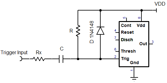
The trigger input is level sensitive. To get the effect of edge triggering, an input RC high pass filter can be used to block the DC value of the trigger source.
Input falling edge pulls trigger voltage down; the trigger voltage will remain low for the lesser of input low time or R * C* ln(1.5) as the capacitor charges. The capacitor will continue to charge with the input low until capacitor voltage is VDD, more specifically (VDD-VIN). When input goes high then the capacitor quickly discharges trough the diode. The diode protects the trigger input from the high voltage that would occur without the diode. A small additional input resistor, Rx, can be used to limit the peak current for capacitor discharge which comes from VIN. This resistor should be less than 1/10th of the VDD resistor to keep the initial trigger voltage low and to keep the timing formula simple.
RESET input effect on mono stable timer
When the reset input goes low, the output will go low immediately. If the output was high, the pulse will be terminated. If the output was low, it will stay low even if a trigger input occurs. The discharge pin will also be low and will keep the timing capacitor discharged. Connect reset input to supply pin when reset feature is not needed. Check data sheet for the low input level.
RESET tied to TRIGGER mono-stable triggering
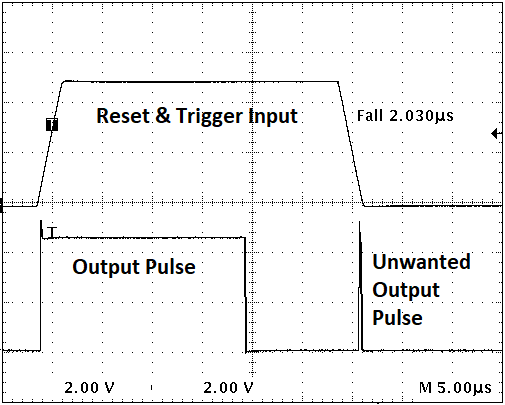
In normal mono-stable setup, the output pulse starts with a low input trigger. Sometimes it is more convenient to have a high trigger level start the output pulse. This option is supported by the bipolar timers; the CMOS timers may not trigger on input high and may glitch on input falling edge. With reset and trigger pins tied together, a low input asserts the reset state making the output low. When the input pair goes high, the reset request stop first and trigger’s low level stops shortly after that. The storage delay of the trigger comparator also helps to ensure a reliable trigger. The timing capacitor will charge to 2/3 of the supply voltage tripping the threshold comparator ending the pulse just like the normal setup. The output and discharge pins will then go low at the end of the pulse.
Unlike the normal mono stable setup, the input trigger / reset signal must be longer than the timing pulse. When the input goes low, the output will go low whether or not the output was high (still running) or low (timing already complete). The input must return low to prepare for the next input high trigger event. The input rising and falling edges should be quick, less than 1µs, to prevent an output glitch when reset / trigger returns to input low.
Output glitch due to trigger/reset input falling too slowly
Control voltage
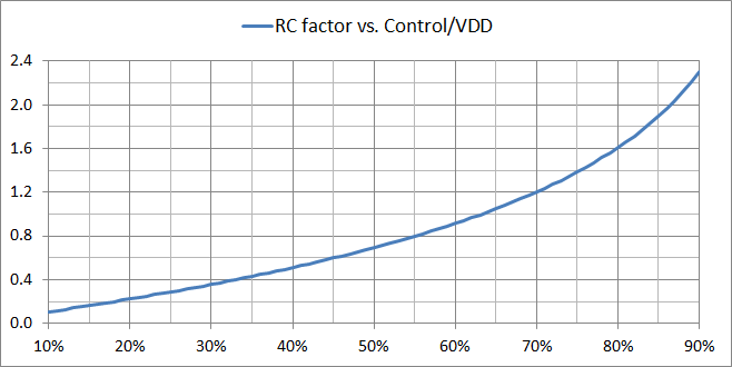
The control pin voltage is internally generated and is normally 2/3 of the supply voltage. A capacitor on the control pin to ground will help filter out supply noise for the comparator internal level. The control voltage can be forced to a different voltage. The new peak capacitor voltage that ends the output pulse will be same value as control voltage and the trigger input comparator point will be ½ of the control voltage. Pulse time will vary with control pin voltage. Pulse time is RA * C * -Ln (1-VCONT/VDD). This formula becomes increasingly non –linear as the control voltage increases.
Time RC constant [-Ln (1-VCONT/VDD)] vs. Control voltage ratio [VCONT/VDD]
Peak discharge Current
An optional resistor placed in series with the timing capacitor can be added to limit the peak discharge current. With no resistor, the peak current is limited by the discharge transistor characteristics and capacitor equivalent series resistance. All timers can tolerate this peak current. Larger capacitors store more energy so using a series resistor with large capacitors could be helpful, but it is not required. The peak current for the CMOS timers when operated above 4V can be several hundreds of milli-amperes. The bipolar timers have less discharge drive. If desired, the discharge current can be reduced to a value set by a series resistor, Rx. Peak current with resistor is less than (2 * VDD) / (3 * RX).
Bypass capacitance
The CMOS and LM timers recommend that two bypass capacitors be used; 100nF ceramic and 1uF electrolytic. Bypass capacitance is more important when the mono stable pulse time is long to prevent output high glitch just after the pulse end. The NA, NE, SA, SE timers recommend at least 100nF.


