This thread has been locked.

If you have a related question, please click the "Ask a related question" button in the top right corner. The newly created question will be automatically linked to this question.

LMX2594: LMX2594 to HMX987 interconnction

Part Number: LMX2594
Other Parts Discussed in Thread: ADC12DL3200

Dear Sirs,

in my design I use four ADC12DL3200s. The ADC clocks are generated with the following chain:

- source LMX2594;
- buffer 1:4 HMC987;
- switch NB7V72MMNG (one for each ADC12DL3200);
- div2 NB7L32M the output is connected to the ADC12DL3200 clock input.

The switch NB7V72MMNG selects the clock source between the internal source (LMX2594+HMC987)
or an external clock.

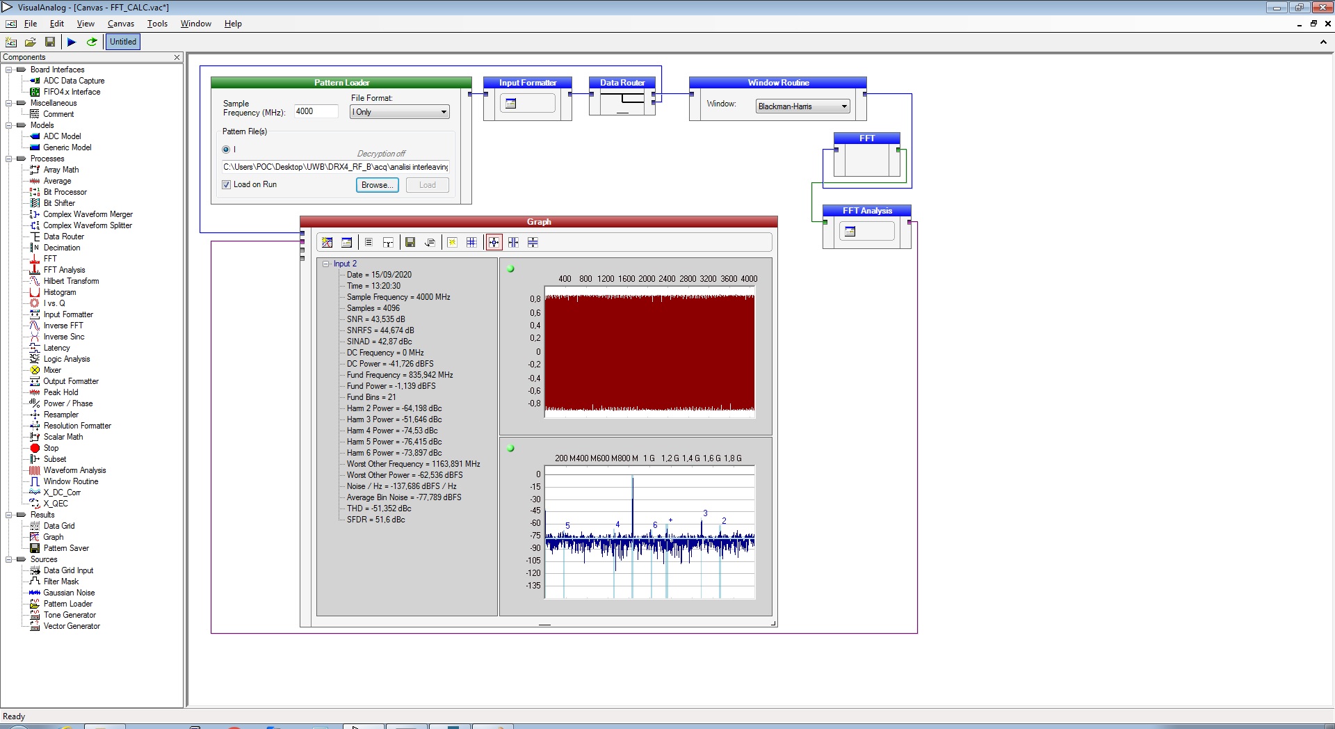
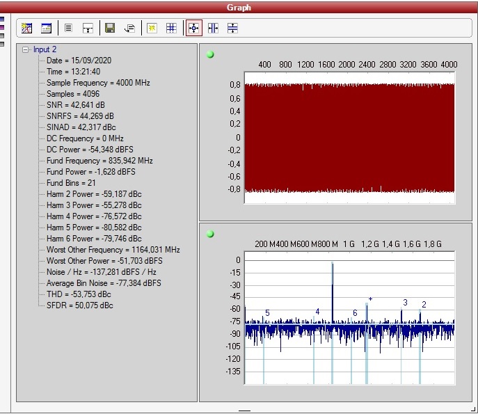
In this configuration, when I generate a 4 GHz clock and then select with the NNB7V72MMNG
the internal source, the ADC12DL3200s work correctly but they generate also  an interleaving spurious
(clock or Gain). Usually this spurious have a power between the -45 and -60 dBFs.

When I select with the NB7V72MMNG an external source generated by a RF instrument
(always 4 GHz), the interleaving spurious there aren' t.

If I re-calibrate the PLL this interleaving spurious can change the values -45 to -60 dBFs (also
If I re-power on the board), while when I re-calibrate the ADC, the spurious power are the same.

One of the possible source of this spurious is the interconnection between the PLL LMX2594 and
and the HMC987. The two components have an A.C. coupling, the LMX2594 have a 50 Ohm to 3.3
and the HMC987 input has an internal termination: PECL termination and 50 Ohm.

Do you have any suggestions about the origin of the interleaving spurious?

Could you help me to understand why the ADC12DL3200 generates the interleaving spurious?
Are there specific conditions to have these types of spurious (for example the clock is non symmetric
or the duty cycle is not 50%)

Do you think that the LMX2594 work correctly with the HMC987?

Thanks in advance.

Best Regards.

  • Hi Daniele,

    Could you provide a plot showing the interleaving spurs? I am not sure what need to be done here without see the problem.

  • Hi Noel,

    in the following images you can see two FFTs of one ADC channel with and without a interleaving spurious.

    Regards,
    Daniele Sassaroli

  • Hi Daniele,

    I am not familiar with the ADC FFT plot, I cannot tell what was the problem.

    Anyway, I think you have a 100MHz reference clock to LMX2594 and then the output is 4GHz. If this is the case, the VCO will be 8GHz and get divided down to 4GHz. So there are harmonics at 8GHz, 12GHz and so on. Would these harmonics hurt the ADC dbFS?

    In addition, since the reference clock is 100MHz, there will be 100MHz spurs around the 4GHz output, do these spurs matter? Not sure if you have enabled the OSC_2X doubler, disable it and see if there is any improvement. Furthermore, after it is lock, set R2[10] to 0 to disable the internal state machine clock. This should reduce the 100MHz spurs level.

  • Hi Noel,

    It's strange that you are not familiar with the FFT of the ADC data, The ADC12DL3200 is an interleaved ADC
    and these type of ADCs produces two type of spurious in the FFT data. Maybe your an not specialist
    of this type of ADCs.

    In my design I'm using a PLL with a 20 MHz reference clock and surely I'll follow your suggestions.

    However I've with to understand why the ADC12DL3200 with one input (in DES mode) generates the interleaving
    spuorious despite the internal calibration procedure.

    Daniele Sassaroli
     

  • Hi Daniele,

    Our team do timing and clocking product, for ADC question, please make a post to the data converter forum, 

    Let us know if the suggested change to LMX can fix the interleaving spurs issue, it will be a good learning to us.

    If you follow up questions on the LMX devices, continue to post it here. Thank you.