This thread has been locked.

If you have a related question, please click the "Ask a related question" button in the top right corner. The newly created question will be automatically linked to this question.

LMK04832EVM: LMK04832EVM

Part Number: LMK04832EVM
Other Parts Discussed in Thread: LMK04832, ADS54J60, PLLATINUMSIM-SW, TICSPRO-SW

HI,

I am now testing the evaluation board of the LMK04832 device.

I want to connect it to a spectrum analyzer to measure its phase noise.but the outputs of the PLL are not RF. They are PECL, LVDS, CML or LVCMOS.

How should I connect the output to a spectrum analyzer to measure phase noise?

Thanks,

Yuval

  • HI,

    One more question.

    If i want to connect the LMK04832 device to more than 7 JESD204B devices (working at subclass 1) and I want that the clock to all devices will be 0 phased synchronized. How would you recommend me to do it?

    Yuval

  • HI,

    In my design I plan to connect the LMK04832 CLK out to the A2D ADS54J60.

    I read in the PLL data sheet that the clock delay+divider can be bypassed (section 8.1.9.2). This will give me high performance. The problem is that In this mode, the only usable output format is CML

    The ADS54J60 clock inputs format is LVDS, LVPECL or Sine wave (all AC coupled) - no CML is mentioned.

    Can't I use the CML PLL clock output to the A2D ? 

    Yuval

  • Hi Yuval,

    Yuval Minster said:
    How should I connect the output to a spectrum analyzer to measure phase noise?

    You have a few options:

    • Use a balun to convert differential to single-ended (LVDS, HSDS, PECL, CML, LVCMOS).
    • AC-couple the differential pair, connect one single-ended leg of the pair to the SpecAn, and terminate the other leg to 50Ω (PECL, CML, LVCMOS). It is technically also possible to do this with LVDS or HSDS, but not recommended, since LVDS/HSDS are intended to be differential all the way to their termination.

    Yuval Minster said:
    If i want to connect the LMK04832 device to more than 7 JESD204B devices (working at subclass 1) and I want that the clock to all devices will be 0 phased synchronized. How would you recommend me to do it?

    We have many suggestions for synchronizing multiple devices in the Multi-Clock Synchronization application note and accompanying slideset. Please review this material first.

    Yuval Minster said:
    Can't I use the CML PLL clock output to the A2D ? 

    Technically, the maximum frequency to the ADS54J60 is only 1000MHz, so unless you plan to use the LMK04832 in distribution mode, high performance CML bypass mode will only operate at frequencies above the usable clock frequency of the ADS54J60. Furthermore, below 250MHz, LVPECL and CML noise floor performance are equivalent.

    If you do plan to use distribution mode for a clock above 250MHz to the ADS54J60, the CML clock amplitude will be effectively equivalent to the LVPECL amplitude. As long as you AC-couple the CML clock (a configuration which is endorsed by the ADS54J60 datasheet in figure 148), connecting a CML clock to the ADS54J60 is acceptable.

    Regards,

  • Hi Derek,

    I am trying to work with the LMK04832 evaluation board but until now with no success.

    For the beginning i just wanted to see a clock at the output by scope but for some reason i do not see anything.

    This is what i did:

    1. I connected a 122.88MHz, 5dBm sine wave to CLK1

    2. I used the TICS to program the device to the default values.(the clock distribution is 2949.12MHz) 

    3. The LED is on so i know that the PLL is locked

    4. I programmed Clock out 9 to be active, CMOS (Norm/Norm) and set it to ~134M by changing the divider to 22.

    5. I connected the output to a scope but i don't see any signal

    Do you know what i did wrong?

    Yuval

  • Hi Yuval,

    Can you save the configuration you tested as a .tcs file using TICS Pro "File -> Save" menu, and post it for review?

    Regards,

  • Hi Yuval,

    CLKout8_9_PD must be set to 0 (unchecked) to power up CLKout9.

    Regards,

  • Hi,

    I unchecked the PD pin and i now see a CMOS signal at the output.

    I have few more questions:

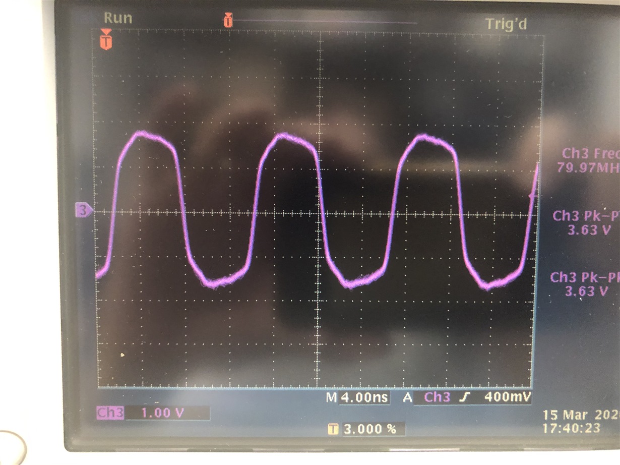
    1. the CMOS output does not looks good (bad SI), see attached. Is it because the 240 ohm to GND ?

    2. I changed the output to PECL or CML but in this case i do not see any signal on the scope. Do you know why?

    Yuval

  • Hi Yuval,

    The default CLKout9 configuration does not have any external termination, just AC-coupling capacitors. The LVCMOS signal is not being corrupted due to alternate termination. In my experience, LVCMOS over long cable runs and with no series damping tends to see distortion like what is pictured above. If you can reduce the distance traveled by the LVCMOS signal to the oscilloscope, or add a small series resistance (e.g. a 3dB pad), you should see the quality of the signal improve somewhat. Also, I'm not sure what bandwidth your oscilloscope has; I suspect it should be sufficient to monitor an 80MHz signal, but it is worth double-checking that your bandwidth is about 5x the highest frequency observed, to ensure your edges are not distorted due to higher order harmonic losses.

    Because there's no termination on CLKout9 by default, there's no way a PECL or CML termination would work on CLKout9 - you must install PECL termination (e.g. 240Ω to GND, or 50Ω to VCC - 2V) to get PECL output, or CML termination (50Ω to VCC, or 68nH + 2x20Ω to VCC for slightly improved EVM/bondwire matching) for CML output.

    Regards,

  • Hi,

    I understand my mistake. I looked at CLK0 in the design and since it has a 240 ohm resistor to GND, I assumed that all channels are the same. Since it isn't, i looked at CLK0 and saw a LCPECL clock.

    I connected it to Spectrum analyzer (Rohde and Schwarz model FSW) and measured 3 types of frequencies: 737.28M, 1474.56M and 2949.12M.

    I measured phase noise (1KHz to 10M offset) and insert the results to a "phase noise to jitter calculator".

    The calculator gave me 3 results: phase jitter, period jitter and cycle-cycle jitter

    For the 737.28M the results were: phase jitter 75fs, period jitter 100fs and cycle-cycle jitter 180fs

    For the 1474.56M the results were: phase jitter 78fs, period jitter 140fs and cycle-cycle jitter 250fs

    For the 2949.12M the results were: phase jitter 1.082ps, period jitter 18.5ps and cycle-cycle jitter 32.06ps

    1. When you write in the data sheet RMS jitter do you mean phase jitter, period jitter or cycle-cycle jitter

    2. My jitter results are worst than yours and it increases as I increase the CLKout frequency. What do you think is the reason for that (the spectrum analyzer should not be the problem)

    Yuval

  • Following the previous reply, I did not mention it but for the reference clock (which is connected to CLKin1) I use the Rohde & Schawrz SMC100A signal generator. it is set to 122.88M, 5dBm

    Also, Attached my tcs configuration

    Yuval

    CLKOut0_2949M_LVPECL.tcs

  • HI,

    Sorry for the many messages. I think that i found the problem of the 2949.12MHz worst jitter. To get this frequency I had to set the clock divider to 1 and i did not set the duty cycle correction bit. Therefore the results were bad. When I set this bit to '1' i got better results but still not the same as in the datashhet and i still see degradation in jitter as the frequency increases.

    For the 2949.12M the results were: phase jitter 142s, period jitter 230fs and cycle-cycle jitter 400fs

    I want to summarize my questions:

    1. Why I do not get the same jitter results as you get ?

    2. What exactly the duty cycle corrections does ?

    3. When I divide 2 output clocks by 2 for example, will they have the same phase or can they have 180 degrees between them

    4. When I divide an output clock by 2 for example, after power off & on will the output keep the same phase or is it possible that I will have 180 degrees difference between one power up cycle to another?

    5. When you write in the data sheet RMS jitter what kind of jitter do you refer to ? phase jitter, period jitter or cycle-cycle jitter, something else ? (when I inserted your phase noise result from figure3 in the data sheet i got the following results: phase jitter 62s, period jitter 60fs and cycle-cycle jitter 100fs. So I guess that RMS jitter in the datasheet refers to phase jitter

    Thanks,

    Yuval

  • HI,

    I tried to connect to the ref clock a clock of 12.288M instead of 122.88M.

    I changed the R of PLL1 to 12 and i thought this should work.

    Unfortunately i see that PLL1 Digital Lock Detect LED is off.

    I do not understand what did I do wrong.

    Please explain.

    Attached tcl file

    Thanks,

    Yuval

    ref clock 12_288M.tcs

  • Hi,

    Any update?

    Thanks,

    Yuval

  • Hello Yuval,

    1. Why I do not get the same jitter results as you get ?


    The jitter we measure in the datasheet is for frequency offsets 12 kHz to 20 MHz. Is this the same band you are measuring. The exact jitter measured will also depend on the phase detector frequency you are using, VCO frequency as well as divider used. The higher the phase detector frequency the better the PN. You can simulate the phase noise on the PLLATINUMSIM-SW.

    2. What exactly the duty cycle corrections does ?

    The duty cycle correction is supposed to help with a cleaner 50-50 clock signal. This setting is specifically required when a divider value of 1 is used. "Both even or odd divides output a 50% duty cycle clock if duty cycle correction (DCC) is enabled."

    3. When I divide 2 output clocks by 2 for example, will they have the same phase or can they have 180 degrees between them

    They may or may not have the same phase, you may need to synchronize the outputs.

    4. When I divide an output clock by 2 for example, after power off & on will the output keep the same phase or is it possible that I will have 180 degrees difference between one power up cycle to another?

    They may or may not have the same phase, you may need to synchronize the outputs. Please take a look at the app note: SNAA294.

    From the app note:

    "This phase uncertainty is caused when dividers start dividing the reference input frequency at different edges, or when the initial state of the dividers may have a different starting values at power up."

    5. When you write in the data sheet RMS jitter what kind of jitter do you refer to ? phase jitter, period jitter or cycle-cycle jitter, something else ? (when I inserted your phase noise result from figure3 in the data sheet i got the following results: phase jitter 62s, period jitter 60fs and cycle-cycle jitter 100fs. So I guess that RMS jitter in the datasheet refers to phase jitter

    "I tried to connect to the ref clock a clock of 12.288M instead of 122.88M.

    I changed the R of PLL1 to 12 and i thought this should work.

    Unfortunately i see that PLL1 Digital Lock Detect LED is off.

    I do not understand what did I do wrong."


    Can you try changing your PLL1 R Divider and PLL1 N Divider to say 1 and 10. A higher phase detector frequency may solve the problem. You will also need to toggle RESET R0[7] and load all registers when you make changes to the PLL.

    Thanks,

    Vibhu

  • HI,

    Thank you for your answers. Sorry for the many questions that I have but this is the 1st time I am working with JESD204B.

    I will try to explain my new project. In my project an analog signal is transmitted to several ADC. Each ADC samples at very high frequency (the frequency will be 1-3GSPS). The outputs of the ADCs will be connected to FPGA for diagnostic. My plan is to use the LMK04832 as a clock and SYSREF generator.

    My questions are:

    1. I understand that if I use a clock divider > 1 then i need to synchronize between the Dev clock outputs. Is it true also if the clock divider = 1 ?

    2. I do not understand why if clock divider = 1, I need to set the DCC flag. To my understanding, if the clock divider = 1 then it is like a buffer, therefore if the ref clock and the VCO has a 50% duty cycle then why do I need to set the DCC? shouldn't the device clock be also 50% duty cycle?

    3. Regarding the SYSREF. I tried to work with the eval board and I have few questions:

    a. Each ADC + FPGA should get a SESREF signal. Should they all be synchronized to the same clock edge? if yes which clock ?

    b. I saw in the data sheet that I need to adjust the SYSREF delay (analog + digital) in order to keep the setup+hold time constrain. I do not understand how this should be done in reality and why the PLL does not take care of it. In general, what is the method (if required) to synchronize two SYSREFs ?

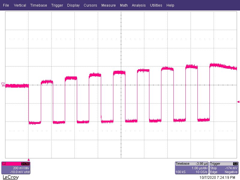
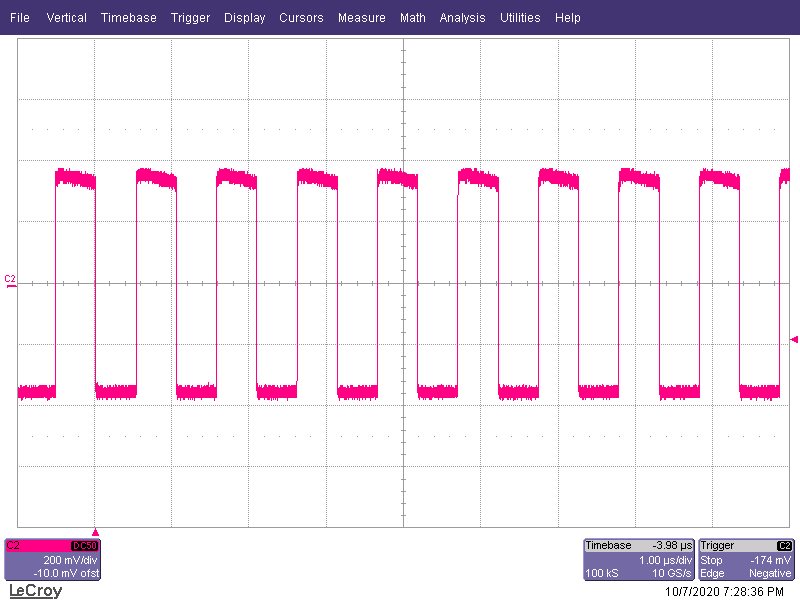
    c. I connected the SYSREF of CLK1 output (set to LVPECL 2V) to a scope and ran it in two modes: continuous and Pulse. I have also few questions about this:

    i. It looks like the signal at the output charging a capacitor cause I see the signal amplitude increases over time (it can be easily seen at the pulse mode). In the continuous mode you can see how at the end the signal stabilize. Is it because the eval board ? the PLL chip? (see attached pictures)

    ii. I tried to operate  the SYSREF by changing the polarity of SYNC_POL but it did not activate the pulser. What did I do wrong. The only way to activate the pulser is by pressing the "Send Pulses" button in the SYNC/SYSREF window.

    Thanks for the assistance ,

    Yuval

  • Hi Yuval,

    Yuval Minster said:
    1. I understand that if I use a clock divider > 1 then i need to synchronize between the Dev clock outputs. Is it true also if the clock divider = 1 ?

    If the clock divider is 1, no synchronization should be required (as long as all clocks have the same half-step setting).

    Yuval Minster said:
    2. I do not understand why if clock divider = 1, I need to set the DCC flag. To my understanding, if the clock divider = 1 then it is like a buffer, therefore if the ref clock and the VCO has a 50% duty cycle then why do I need to set the DCC? shouldn't the device clock be also 50% duty cycle?

    The LMK04832 distinguishes between "bypass mode" which routes the clock distribution path directly to the CML output buffer (bypassing all the potentially noise-generating dividers, muxes, and other circuitry), and the "divide-by-1" mode. We don't have a mux that just bypasses the divider, because adding another mux would end up hurting phase noise performance more than just running through the divider circuit.

    For odd divide values (including divide-by-1), the divider needs to have insight into both the rising and falling edge of the clock distribution source to properly coordinate rising and falling output edges; enabling DCC switches the circuit to use both rising and falling edge timings.

    Yuval Minster said:
    3a. Each ADC + FPGA should get a SYSREF signal. Should they all be synchronized to the same clock edge? if yes which clock ?

    In JESD204B, your clock generator sends out a SYSREF pulse to all devices in the system simultaneously. There may be some minor offset or skew between these devices due to routing length differences, board placement, etc, but the LMK04832 and similar JESD204B clock generators can be used to trim out that skew to ensure deterministic device clock to SYSREF alignment for every device across power cycles.  Even if there's a nanosecond of skew difference between two clocks on the board, such that one device receives its device clock and SYSREF 1ns later than another, as long as that nanosecond of skew is repeatable between power cycles it can be calibrated out. But if the SYSREF edge timing changes by ±1 device clock cycle, the skew is no longer deterministic: maybe one device started counting a few hundred picoseconds early, or a few hundred picoseconds late.

    Each ADC + FPGA uses the SYSREF edge as the signal to "start counting", so in a sense they are synchronized to that SYSREF clock edge.

    Yuval Minster said:
    b. I saw in the data sheet that I need to adjust the SYSREF delay (analog + digital) in order to keep the setup+hold time constrain. I do not understand how this should be done in reality and why the PLL does not take care of it. In general, what is the method (if required) to synchronize two SYSREFs ?

    The PLL does not know how long your board traces are. If you cannot match the length of your device clock and SYSREF traces, or if there are multiple LMK04832 which must be synchronized, the PLL cannot figure out by itself what the appropriate delay settings are.

    In practice, you align your device clock edges in 150-200ps coarse steps using the digital delays and half-step, and control the routing lengths to ensure that the edge timing of the device clock on each target device aligns as closely as possible. Then the SYSREF divider output is delayed globally by some number of VCO cycles, and again locally by analog and digital delays on a per-output basis, to ensure the SYSREF edge meets setup and hold requirements for each target device.

    If every clock output and SYSREF has the same routing length, AND every device clock is the same frequency and digital delay value, AND every device clock is synchronized (along with the SYSREF divider) at the same time, then only the SYSREF global delay is required to place the SYSREF edge at the falling edge of the device clock. But if the routing lengths are different to some devices, or if there are multiple frequencies e.g. 491.52MHz and 245.76MHz, the local digital delays will need to be different to ensure the same edge timings for every device clock, and the local SYSREF digital delays may need to be different to place each SYSREF edge at a particular falling edge on each device clock (since the different frequency clocks no longer share the same setup and hold time/falling edge).

    At 3GHz, routing length discrepancies or even output-to-output skew may be enough to violate setup and hold time for the SYSREF edge, beyond what digital delay in 150-200ps steps could correct. So at very high frequencies, compensating SYSREF edge timings with analog delay can help. Also over temperature, some shift in output skew can occur, which can be calibrated using the analog delays.

    Yuval Minster said:
    3ci. It looks like the signal at the output charging a capacitor cause I see the signal amplitude increases over time (it can be easily seen at the pulse mode). In the continuous mode you can see how at the end the signal stabilize. Is it because the eval board ? the PLL chip? (see attached pictures)

    The eval board has AC-coupling capacitors on the SYSREF path.

    Yuval Minster said:
    3cii. I tried to operate  the SYSREF by changing the polarity of SYNC_POL but it did not activate the pulser. What did I do wrong. The only way to activate the pulser is by pressing the "Send Pulses" button in the SYNC/SYSREF window.

    If you click "Send Pulses" you'll note the SYNC_MODE mux is set to SYNC SPI (pulser) mode. If you want SYNC_POL toggle to trigger SPI pulses, you need to set SYNC_MODE mux to SYNC Pin (pusler) mode.

    Regards,

  • Hi Derek,

    Thanks for your detailed answers. I still have some more questions and need more clarifications from you. I attached a high level block diagram that will help to understand my future design.

    Your assumptions are correct. The clock to all ADCs is the same and I do not see any problem to keep the same routing in length for each clock and SYSREF. Take into consideration that since some ADCs samples the same input then I need to use subclass 1 in order to synchronize them.

    My questions are:

    1. What did you mean in your answer when you say "AND every device clock is synchronized (along with the SYSREF divider) at the same time" ?

    2. If the clock and SYSREF to each ADC is routed identical but the routing between the ADCs are different, is it still OK (from your answer, I understand it is)?

    3. I understand that the SYSREF resets all the counters therefore although the ADCs might transmit the same samples at different times (because the SYSREF for each ADC might arrive at different time), the FPGA should know how to handle it. I still do not understand why the FPGA need to get a SYSREF signal (I saw that in subclass 1, this is how it should be done). Isn't it enough that the ADCs receive the SYSREF? why the FPGA should receive it too? 

    4. If the clock + SYSREF routed identical to the ADC, do I still need to synchronize between the SYSREF to the falling edge of the clock? does the PLL has a default timing relation between the SYSREF to the clock?

    5. If the answer for (4) is yes, I still do not understand how I know when the SYSREF is synchronized to the falling edge of the clock. Is there a procedure to align between the SYSREF to the clock?

    6. In case that I need to use 2 PLLs and they get the same ref clock. Does it change something in the alignment procedure between the SYSREF and the clocks?

    7. In the data sheet of the PLL, section 8.3.5, ("SYSREF to Device Clock Alignment" ) describes how to align the SYSREF to the clock. It describes how to calculate the SYSREF_DDLY (SYSREF global delay) value.

    a. Is this the method that I should use to synchronize the SYSREF to the clock?

    b. In table 3, I do not see what should be the value of DCLK_DIV_ADJUST when DCLKX_Y_DIV = 1

    c. In the example of this section, I do not understand why SCLKX_Y_DDLY = 2. The minimum value is 8 so why in this example the SCLKX_Y_DDLY equals 2 ?

    Thanks,

    Yuval

    Data path HL block diagram.docx

  • Yuval Minster said:

    1. What did you mean in your answer when you say "AND every device clock is synchronized (along with the SYSREF divider) at the same time" ?

    I believe Derek was trying to say that if all the device clocks have the same frequency and all the device clock traces to the receivers are the same length, the device clocks would then have the same rising edges. Additionally if all the SYSREF are also the same frequency similarly all have the same rising edges then all you need to do is use the global SYSREF delay to "place the SYSREF edge at the falling edge of the device clock".

    Yuval Minster said:

    2. If the clock and SYSREF to each ADC is routed identical but the routing between the ADCs are different, is it still OK (from your answer, I understand it is)?

    Yes this is okay. You would align your device clocks with the digital delay and half steps and then adjust the SYSREFs using their analog and digital delay. Each device clock and each SYSREF has its own digital delays, unless an output pair is configured to be two device clocks or two SYSREFs.

    Yuval Minster said:

    3. I understand that the SYSREF resets all the counters therefore although the ADCs might transmit the same samples at different times (because the SYSREF for each ADC might arrive at different time), the FPGA should know how to handle it. I still do not understand why the FPGA need to get a SYSREF signal (I saw that in subclass 1, this is how it should be done). Isn't it enough that the ADCs receive the SYSREF? why the FPGA should receive it too? 

    The SYSREF is a timing reference that is used by all devices in the link. All the devices need to be synchronized by the SYSREF. The SYSREF is related to the frame clock and helps generate all the sample clocks and LMFCs in the system. There is a detailed TI video training series that goes over the JESD204B standard. You can find the training here:

    Yuval Minster said:

    4. If the clock + SYSREF routed identical to the ADC, do I still need to synchronize between the SYSREF to the falling edge of the clock? does the PLL has a default timing relation between the SYSREF to the clock?

    Yes, you will still need to do this. However, as Derek mentions, it will be a lot simpler and you can do it with just the global SYSREF delay.

    Yuval Minster said:

    5. If the answer for (4) is yes, I still do not understand how I know when the SYSREF is synchronized to the falling edge of the clock. Is there a procedure to align between the SYSREF to the clock?

    Please see “8.3.3.1.1 Setup of SYSREF Example” and “8.3.5 SYSREF to Device Clock Alignment” sections of the datasheet, as well as the app note and slide deck Derek has pointed you to earlier in his Sept 16th post to this thread. The sections in the datasheet provide equations to calculate the delays.

    Yuval Minster said:

    6. In case that I need to use 2 PLLs and they get the same ref clock. Does it change something in the alignment procedure between the SYSREF and the clocks?

    You will need to ensure that in addition to the same reference the SYNC event also occurs at the same time in both devices. This will ensure the outputs from both LMK04832s with the same frequency have the same rising edge provided the traces are the same. You can also use 0-delay depending on your frequency plan. The slides do a good job explaining what your options are.

    Yuval Minster said:

    7. In the data sheet of the PLL, section 8.3.5, ("SYSREF to Device Clock Alignment" ) describes how to align the SYSREF to the clock. It describes how to calculate the SYSREF_DDLY (SYSREF global delay) value.

    a. Is this the method that I should use to synchronize the SYSREF to the clock?

    b. In table 3, I do not see what should be the value of DCLK_DIV_ADJUST when DCLKX_Y_DIV = 1

    c. In the example of this section, I do not understand why SCLKX_Y_DDLY = 2. The minimum value is 8 so why in this example the SCLKX_Y_DDLY equals 2 ?

    7.a. This is the method to determine the delays and associated register settings needed to create the right alignment between the device clocks and SYSREFs.

    7.b. I will need to get back to you on this.

    7.c. I believe you are confused between SCLK_X_Y_DDLY and SYSREF_DDLY. SYSREF_DDLY is the global SYSREF delay and has a minimum value of 8. SCLK_X_Y_DDLY is the local SYSREF delay common to a single output pair and can be bypassed, or set to a value between 2 and 11 cycles.

    Thanks,

    Vibhu

  • Hi Vibhu,

    Thank you for your answers. I still do not understand perfectly the example in section 8.3.5 (SYSREF to Device Clock alignment).

    This equation helps you to define the SYSREF_DDLY in order to get an alignment between the SYSREF and the DEVCLK.

    In the equation there is a parameter called SCLK_X_Y_DDLY which in the example equals 2.

    According section 8.6.2.2.7 in the datasheet this parameter can have a minimum value of 8. The parameter SCLK_X_Y_ADLY (section  8.6.2.2.6) can get values from 0 to 15, as you said in your answer but it is ADLY and not DDLY and ADLY is not part of the equation. Please explain what I miss?

    Also, how did you choose the 2 value for this parameter?

    Thanks,

    Yuval

  • Hello Yuval,

    SCLK_X_Y_DDLY is a digital delay specific to an output pair. It can be bypassed or set to be between 2 and 11 SYSREF clock cycles.

    SCLK_X_Y_ADLY is an analog delay specific to an output pair. It ranges from 125 ps to 608 ps in steps of ~21 ps.

    SYSREF_DDLY is a global digital delay applied to all SYSREF outputs. SYSREF_DDLY > 7.

    It may be helpful to take a look at the device in TICSPRO-SW.

    Thanks,

    Vibhu

  • HI Vibhu,

    Thanks for the answers.

    1. I understand what SCLK_X_Y_DDLY and SCLK_X_Y_ADLY mean and I see that in the TicsPro I can change the SCLK_X_Y_DDLY from 2-11 cycles. I was confused from the datasheet description (but now I think I understand it). In table 8.6.2.2.7, the description of the SCLK_X_Y_DDLY says "Set digital delay value for SYSREF clock (minimum 8)". Does "minimum 8" means that the minimum clock delay is 8 ?

    2. I have an open question that I still did not get an answer from you. In table 3, I do not see what should be the value of DCLK_DIV_ADJUST when DCLKX_Y_DIV = 1

    Thanks,

    Yuval

  • Hello Yuval,

    Yuval Minster said:
    In table 8.6.2.2.7, the description of the SCLK_X_Y_DDLY says "Set digital delay value for SYSREF clock (minimum 8)". Does "minimum 8" means that the minimum clock delay is 8 ?

    I believe that this is a typo. The minimum 8 is for the global sysref delay, SYSREF_DDLY.

    Yuval Minster said:
    2. I have an open question that I still did not get an answer from you. In table 3, I do not see what should be the value of DCLK_DIV_ADJUST when DCLKX_Y_DIV = 1

    I do not have an answer on this yet, I will let you know as soon as I do.

    Thanks,

    Vibhu

  • Hello Yuval,

    Regarding the open question.

    I do not think the DCLK_DIV_ADJUST matters at all when DCLKX_Y_DIV = 1. Any full step adjustment would have the same phase relationship.

    This is probably why it isn't on the datasheet.

    Thanks,

    Vibhu