This thread has been locked.

If you have a related question, please click the "Ask a related question" button in the top right corner. The newly created question will be automatically linked to this question.

LMK04616: Datasheet parameters confuse

Part Number: LMK04616

Dear team

We plan to use the LMK04616 in PLL2 only mode, with OSCin,  for both ZDM  and pure buffer mode. And we have some confuse as below:

1. In ZDM mode, the feedback channel is CH7/8 or CH 6/9?

2. In ZDM mode, and also need to sync all the output divider, will our device support?

3. In ZDM mode, the phase error between input and feedback channel?

4. OSCout will always have same frequency as OSCin in any condition?

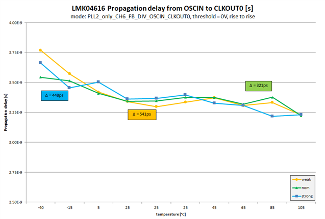
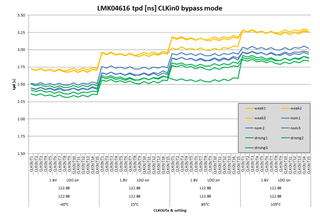
5. In Buffer mode, the OSC in to Clkout propagation delay, Min and Max value?

6. In Buffer mode, the part to part skew, Min and Max Value?

Thanks

Jun Shen 

  • Hello Jun,

    1. For LMK04616, programming PLL2_FBDIV_MUXSEL (0x146[1:0]) can select between either CH6 (=0x2) or CH9 (=0x1).
    2. In ZDM, the output being used for ZDM feedback should not be SYNC'd (as it will have a reproducible phase offset to the input phase). SYNCing the ZDM output can cause the PLL state machine to freeze, requiring a reset. The other outputs can be SYNC'd as normal.
    3. The ZDM phase error depends on the frequency, the R/N divider settings, and the output divider settings. It is better to think of it as introducing a reproducible phase offset with some consistent propagation delay. You do not necessarily know the input to output delay, but you can be sure it should be similar across devices with similar voltage/temperature/layout conditions.
    4. It is possible to route OSCout source from either OSCin or from the PLL2 prescaler output. Additionally, there is an integrated 8-bit divider on the OSCout output which can be used to change the OSCout frequency. In other words, OSCin can be programmed to be the same frequency as OSCout in any condition, but changing the frequency is also possible.

    For the propagation delay and part-to-part skew values, we do not have any min/max values. I have attached some typical data for your review at a specific frequency. Note that, as I said before, changes to the divider settings will change the propagation delay. All measurements are taken with 122.88MHz as the input and output frequency. From the graphs below, buffer mode part-to-part skew looks to be up to 700ps in some cases, whereas ZDM skew appears to be much smaller at up to 30ps.

    Regards,

    Derek Payne

  • Hello Derek

    Thanks for the support, and Now it is more clear.

    1. For the ZDM feedback channel, before we suggest CH7/8 in the GUI, and one of my customer have used this setting in a real system, so this is a typo, or silicon change after the first time we have the datasheet?

    2. If the ZDM feedback channel can not be synced, so if the Fref = Clkfeedback, then all the output will be synced after apply the sync to other clkout?

    3. For the buffer mode, if  part-to-part skew up to 700ps, and the propagation delay is around 2.25ns to 3.25ns from PVT right? so this is for -40deg to 105deg as datasheet mentioned?

    Great thanks

    Jun Shen

  • Hi Jun,

    1. It shouldn't matter if we suggest 7/8 or 6/9, because 6/7 and 8/9 share channel dividers. Functionally choice between 6/9 or 7/8 is equivalent.
    2. Since the ZDM feedback channel is in-phase with the input by default, all the outputs will be synced after applying the sync to the other clkouts. There may be some fixed phase offset between the clocks, which can be compensated with the digital and analog delays.
    3. If the datasheet lists a typical value, it's at room temperature unless otherwise stated. The second graph above would be better for estimating part-to-part min/max skew, as it includes weak/strong process corners and temperature (voltage variation is minor due to integrated LDOs).

    Regards,

    Derek Payne

  • Derek

    Thanks, and it is very clear for the skew and delays, but still have some confuse about the ZDM mode.

    1. It is likely only the feedback path have zero delay feature? or all the output can have the zero delay feature after the SYNC?

    2. if the feedback path can not be sync'd, we do care about how all other output channel divider sync with the feedback channel. it is likely when received the sync control, and all the divider except the feedback channel will be reset, and waiting a point to synchronized with the feedback channel?

    3. if the feedback path can not be sync'd, but other channel applied the sync, how to make sure some fixed phase offset between the clocks?

    4. in the datasheet, figure 32 show a SYNC example, how about the parameter of latency1/2, t skew?  and also why DIV by2 aligned with div by1 falling edge?

    5. the use case is input as 50Mhz, and output of 300Mhz, is there some suggestion about the setting in PLL2 zero delay mode? we need all the output rising edge aligned with the reference clock.

    Thanks

    Jun Shen

  • Jun,

    1. While only one output can be explicitly used as the feedback to the PLL in ZDM, you can definitely synchronize the other outputs to align with the ZDM output.
    2. In order to get the other outputs aligned precisely, you will need a SYNC source that has some precise timing alignment with the reference input or the ZDM feedback output. As long as you can time the SYNC event against the input, for example, the dividers should be consistently reset and sequenced by the digital delays to a precise timing. Since the dividers share a source, it will always be possible for all dividers to share an edge within the limits of the channel-to-channel skew.
    3. I think I addressed this in 2., but in case it is unclear: align the SYNC event with the input clock, and use the digital delays on the other clocks to align the feedback clock edge with the other clock outputs.
    4. Latency is the combination of the SYNC event propagating through the dividers, and the digital delays on each channel which mute the output until the delay expires. Minimum latency (i.e. SYNC event propagation) isn't well-characterized, but it should be equal in terms of VCO post-divider cycles across devices with the same programming. So likely it will be easiest to pick a reproducible SYNC timing with respect to the input clock, then manually test digital delay values and measure the phase of the ZDM output and the other clocks until alignment is achieved. After performing this delay tuning once in the lab on a single system, the programming and SYNC timing can be duplicated on all other systems.
    5. The previous discussion focused on aligning all outputs. If you must also align the input edge to the outputs, it's possible that the zero delay output won't precisely align with the input due to some propagation delay diffefence between the input and output circuitry (even though the phase would be constant). The analog and digital delay is brought inside the loop in zero-delay mode, and so it has no impact on the propagation delay differences. In that case, although the ZDM output might not align perfectly with the input, the other outputs could still be made to align with the input instead through the same procedure.

    Regards,

    Derek Payne

  • Derek

    Thanks for this detail help, and just one more confuse.

    1. If do the divider sync firstly, and then change the feedback to ZDM, will all the output divider still sync'd after change the  feedback path?

    2. if Point 1 works to align the Clkoutx and Oscin, compared with the apply SYNC after ZDM for rest Clkout like mentioned above, which one will be better?

    Thanks

    Jun Shen

  • Jason,

    1. The output dividers will be SYNC'd, but if the N-divider is greater than 1 then the N-divider will not be SYNC'd. There is no way to trigger an N-divider synchronization at a specific time. If the N/R value (N-divider divided by R-divider) is an integer, then there shouldn't be any issues as the reference clock edge will always be aligned to a clock output edge. But if N/R is not an integer, it will not be possible to guarantee that an edge of the output clock aligns with an edge of the reference clock after the switch (since there is no way to reset the N-divider at a precise time). 
    2. Changing the feedback source during operation is somewhat risky. The PLL uses the feedback divider input to the PFD as a state machine clock, and changing the clock without following the proper reset procedure could cause the digital state machine to enter an unknown state requiring a reset. I would strongly recommend applying the SYNC after ZDM for the other CLKOUTs instead.

    Regards,

    Derek Payne

  • Derek

    Great thanks, and we almost finished the design, and there have some confuse for the finally solution.

    1. The SYNC timing, it seemed when set the SYNC as high, the output clock divider will be reset, and when the SYNC is low, the output clock divider will start counting. The SYNC is sampled by the pre scaled clock right? so is there some set and hold timing requirement for the SYNC? and after we set the SYNC as low, the divider will start immediately or there have some fixed delay(except the programed fixed delay)?

    2. if we do not using the ZDM mode, will our device possible to make the Clkout align with OSCin only with SYNC?

    thanks

    Jun Shen

  • Jun,

    1. We haven't evaluated the setup/hold time on the SYNC pin. In practice, I have found that the setup time is <100ps. Hold time is unknown, but at a minimum I recommend using a SYNC pulse that is at least one pre-scaler clock cycle wide. A single pre-scaler edge is sufficient to latch the SYNC signal.
    2. It should be possible to align OSCin to CLKout open-loop (without using ZDM), but because of part-to-part variation and temperature variation it is not guaranteed that the same settings will always generate the same alignment. Some amount of calibration would be necessary to trim out part-to-part variation, and the output delay would have to be adjusted over temperature (perhaps by using the analog delays).

    Regards,

    Derek Payne

  • Derek

    Thanks for the quick support, and for the point2, yes, we understand there will have some part to part variation like you have shared the PVT results. And how about the ZDM mode for the feedback? in this mode, will the zdm feedback make the part to part variation smaller than open-loop mode?

    Thanks

    Jun Shen

  • Hello,

    In general the buffer only configuration will have the lowest variation.

    73,
    Timothy

  • Timothy

    Thanks for the confirmation, and last time we mention one point about how to sync all the output in ZDM mode.

    1. firstly put the device into the normal feedback mode, and sync all output divider.

    2. then switch the device into ZDM mode with CH6 feedback, both R/N are 1.

    3. then re doing the device start to start the PLL.

    we think this will make all output divider SYNC'ed because the VCO is continue running and the divider continue counting , and also the PLL will working  properly after re do the device start?

    This is really important because if this mode works, the will have more timing margin because the delay will not include the sync timing delay.

    if above mode can not support, customer need to change the clock tree solution.

    Thanks

    Jun Shen

  • Jun,

    Since R/N are both 1, I think steps 1 and 2 should be sufficient. I verified in the lab that you do not need to redo the device start after switching into ZDM mode with CH6 feedback, you just have to update the feedback path and the N-divider value. The PLL will re-acquire lock from the feedback path once the N-divider is set to 1 for ZDM feedback, and the outputs remain synchronized since the VCO is still running.

    Regards,

    Derek Payne