This thread has been locked.

If you have a related question, please click the "Ask a related question" button in the top right corner. The newly created question will be automatically linked to this question.

LMK03318: Questions on output filtering/power, STATUS pins, unused clock input pins, VCO calibration, and crystal selection

Part Number: LMK03318
Other Parts Discussed in Thread: LMK03328

Hello,

 I am working on a brand new design for the TMS320C6678ACYP. Pursuant to a suggestion in an earlier e2e dialogue, I have chosen to use the LMK03318 Clock Generator to provide the clocks for the DSP. It turns out that ROM Option 45 will do everything I need: 100MHz for the CORECLK on Output 0, 100MHz for the DDRCLK on Output 2, and 250MHz on Output 4 for the SRIOSGMIICLK. I have the HW_SW_CTRL pin tied to 3.3V. I have six questions:

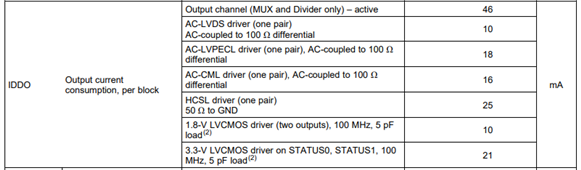
 1)  Since I am not using the rest of the outputs, do I need to provide the filter networks for all of the VDDO pins, or can I simply connect VDDO_5, VDDO_6, and VDDO_7 to 1.8V directly?

 2)  How much power could I save if I developed a custom program for our application and disabled the outputs for all of the unused clocks?

 3)  With ROM Option 45 what is driven onto the STATUS0 and STATUS1 pins?

 4)  Since I’m only using the 25MHz crystal connected to the SECREF_P and SECREF_N pins, and have no other clock sources, what should I connect to the PRIREF_P and PRIREF_N pins?

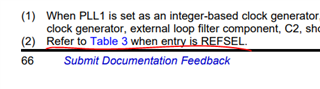
 5)  Is VCO calibration as described on page 42 of the datasheet necessary to meet the phase noise or any of the other requirements of the TMS320C6678ACYP?

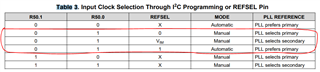
 6)  I have read page 33 of the datasheet, but I don’t know what R50.1 and R50.0 are set to when using ROM Option 45. I have tied the REFSEL pin to VIM. With ROM Option 45 will this force the device to use the secondary crystal input pins manually or will the device automatically select the crystal by itself?

 Best Regards,

Larry

  • Hi Larry,

    1) I think that would be okay as long as they're still connected to 1.8V. (Hao, can you confirm?)

    2) You may use the information on page 9 of the datasheet to estimate how much power you could save by disabling outputs.

    4) Leave PRIREF pins floating and makes sure to disable the buffer by PRIBUFSEL = 0x2.

    5) I recommend calibrating the VCO.

    Hi Hao,

    Please help answer the remaining questions.

    Regards,
    Jennifer

  • Hi Larry,

    For (3), it's LOL1 and LOL2 (Loss Of Lock for PLL1 or 2)

    For (6), the reference selection is decided by the REFSEL pin. See below:

    Regards,
    Hao

  • I was taking snapshots from LMK03328 datasheet instead of LMK03318, but the idea is the same. You can find the information from the same ROM tables.

    Regards,

    Hao

  • Hello Hao,

    Thanks for your help and for Jennifer's also. I have two followup questions below to make sure I understand your reply and Jennifer's reply. 

    I see that Jennifer was asking for your input also on question number 1. What are your thoughts for question #1 about leaving off output power filters for unused buffers?

    Also please provide me with some clarification for my question #4. The reply was that I need to disable the buffer by PRIBUFSEL = 0x2. I was under the impression that I could use the LMK03318 directly for my design without doing any register changes. I have the GPIO pins set to ROM option 45. I have the HW_SW_CNTRL pin tied high. I have the REFSEL pin set to Vim. The 25MHz crystal is connected to the secondary reference input clock pins. What is the problem with using the LMK03318 as I have the hardware pins set if I do not disable the buffer by PRIBUFSEL = 0x2.?

    Regards,

    Larry

  • Hi Larry,

    For (1), yes you don't need to apply supply filtering for VDDO pins of unused outputs. For (4), you don't need to do any register programming. Simply float the unused reference (PRIREF pins) and it'll be fine. 

    Regards,

    Hao

  • Hi Hao,

    Thank you for the additional followup. Just to make sure I understand for the LMK03318, I will set the REFSEL pin to the Vim voltage. Is that correct?

    Regards,

    Larry

  • Hi Larry,

    No you need to pull the REFSEL pin down to select SECREF. Please see Table 3 for more details.

    Regards,

    Hao

  • Hello Hao,

    I am sorry that I did not reply back to you sooner, but I was on vacation last week.

    I think I need more information to understand how the REFSEL pin works when ROM Option 45 is set on the GPIO pins. In looking at Table 3 the options are based on the settings of register bits R50.1 and R50.0. When using ROM Option 45 how are bits R50.1 and R50.0 configured?

    Is there a document that explains all of the register settings for the various ROM Options?

    Regards,
    Larry

  • Hi Larry,

    When the entry is "REFSEL" in the ROM options table, it simply means that the input selection is decided by the status of REFSEL pin. In other words, you should be looking at these three rows: (notice on all the other rows there's "X" on the REFSEL column, meaning that the REFSEL pin status is ignored and that the input selection is determined by registers. ROM options avoid this situation for better flexibility).

    Regards,
    Hao

  • Hello Hao,

    Thank you for the explanation about REFSEL in the ROM options table and pointing me to the relevant entries in Table 3. I still do not understand the primary vs. secondary PLL reference selection. If I look at the relevant entries in Table 3, it seems to me that I should set REFSEL to Vim, as I suggested previously in this discussion. But you told me to set REFSEL low. It seems from the relevant entries in Table 3 that setting REFSEL low will cause the PLL to select the primary PLL reference. Please provide me with an explanation to relieve my confusion. 

    Regards,

    Larry

  • Hi Hao,

    Please recall from the earlier parts of this conversation that for the clock reference I'm only using a 25MHz crystal connected to the SECREF_P and SECREF_N pins. I have nothing connected to the PRIREF_P and PRIREF_N pins, they are floating. 

    Thanks,

    Larry

  • Hi Larry,

    as mentioned in the other post, REFSEL needs to be at VIM to select the secondary input. VIM is typically 0.9V.

    Regards,

    Julian

  • Thanks Julian,

    That makes sense to me about the REFSEL pin.

    I would like to ask a followup question concerning the reply to my original question #5 on the topic of VCO calibration. The reply was that it is recommended, which makes sense, but I would like to have a more detailed explanation please of the consequences of not performing the VCO calibration. Is it really necessary to meet the phase noise or any of the other requirements of the TMS320C6678ACYP? If so, which ones? ls it reasonable to expect that our inital models that are run at room temperature conditions would work? Do we need it for factory volume production? Please elaborate on this topic. 

    Regards,

    Larry

  • Hi Larry,

    yes, you should do a VCO calibration when changing the VCO parameters. The calibration ensures that the optimal phase noise performance is achieved. On top of that the tuning voltage will be set to an optimal point. This prevents potential false lock or unlock events.

    If for example only output dividers or output formats are changed, then a re-calibration is not necessary.

    The calibration is executed automatically at power up. So, if you store the setting in the EEPROM the VCO will be calibrated right after power up.

    regards,

    Julian

  • Hi Julian,

    Thanks, that answers my questions. I did not realize there was a VCO calibration upon power-up. That should take care of it in our application. 

    Regards,

    Larry