This thread has been locked.

If you have a related question, please click the "Ask a related question" button in the top right corner. The newly created question will be automatically linked to this question.

LMK04821: read register

Part Number: LMK04821

According to the standard 3-line SPI reading method, I tried to read the version value 0x006 of LMK04821, but after I sent 0x8006, the last 8 CLKS did not receive the data I needed from SDI. I have verified that the register can be written successfully (after the clock is turned on, Sends 0x01 found clock is off to 0x002). I tried not initializing the clock after system startup and then carrying out the read operation, but it did not work. Is the read operation related to the register configuration at the beginning? The following is my user layer to read the register code.

To simplify my problem: How do I read the register value, ignoring the impact of possible previous register configuration operations on it?

/* set spi mode, bits and speed */
SPI_set_mode(MODE_0);
SPI_set_bits(8_BITS);
SPI_set_speed(1000000);

/* data to be send */
unsigned char tx_buf[] = {0x80, 0x06, 0x00};
unsigned char rx_buf[3] = {0, };
struct spi_ioc_transfer tr = {
		.tx_buf = (unsigned long)tx_buf,
		.rx_buf = (unsigned long)rx_buf,
		.len = 3,
		.delay_usecs = 0
	};
	
ioctl(fd, SPI_IOC_MESSAGE(1), &tr);

  • Shu,

    First, I don't see anything wrong with the mechanics of your SPI transaction in the code snippet above. This looks correct to me.

    Does your SPI controller support 3-wire transactions?

    LMK04821 supports 3-wire readback and 4-wire readback, and can support both simultaneously.

    For 3-wire mode:

    • 3-wire mode is controlled by SPI_3WIRE_DIS field in R0. If SPI_3WIRE_DIS=1, no 3-wire transaction will occur. If SPI_3WIRE_DIS=0, the SDIO pin on LMK04821 will be turned around from input to output on the 16th falling edge of the SPI transaction.
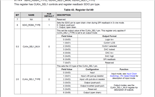
    • SDIO_RDBK_TYPE field controls whether 3-wire SPI uses open-drain or push-pull signaling. The POR default is open-drain (1) so unless there is a pull-up resistor on SDIO, you will not see any signal on the output. If SDIO_RDBK_TYPE=0, the SDIO pin will be set to push-pull mode. Be careful in push-pull mode that there is no bus conflict on the data line.

    For 4-wire mode:

    • One of the GPIO pins (STATUS_LDx, CLKIN_SELx, RESET) must be repurposed for SPI readback by setting the appropriate _TYPE register for that GPIO to SPI readback and setting the output style to one of the open-drain or push-pull options. This transforms the GPIO into the device's SDO pin.
    • Multiple pins can actually be configured as SPI SDO, if for some reason you needed to do this.
    • 4-wire mode can be enabled simultaneous to 3-wire mode as well, if for some reason you needed to do this.

    Double-check that you have either 3-wire or 4-wire configured how you want it, and if you're still encountering difficulty with readback we can troubleshoot further.

    Regards,

    Derek Payne

  • Hi,

    I found this register in the manual, is it the configuration item that determines whether I can read the register? Currently I set 0x149 to 0x42. Does this configuration allow me to configure a register and then run the next command to query its value? I have enabled the third-line SPI

  • If SDIO_RDBK_TYPE=1 (as in your current setting of 0x149), and SPI_3WIRE_DIS=0 (you have not mentioned your register setting for address 0x0, but SPI_3WIRE_DIS=0 i.e. enabled is the default) the SDIO pin will be turned into an open-drain output after 16 clock cycles. The rreadback result will be driven by SDIO pin, but only if there is a pull-up resistor from SDIO to VCC, and only if your SPI controller also disables its output driver on SDIO and becomes a high-impedance input that can read back SDIO from LMK04821.

  • My problem has been solved. Thank you for your assistance