This thread has been locked.

If you have a related question, please click the "Ask a related question" button in the top right corner. The newly created question will be automatically linked to this question.

LMK04208: LMK04028

Part Number: LMK04208
Other Parts Discussed in Thread: LMX2594

I need help with my LMK04208 circuit. I cannot get PLL1_LOCK.


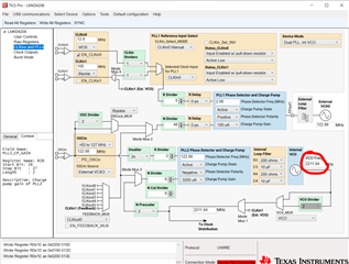
I designed my own PCB based on the Xilinx ZCU111 and the XCZU28DR RFSOC. My LMK04208 circuit is almost identical the ZCU111 circuit with the exception of the TCXO and VCXO components. My VCXO is an Epson VG-4513CA 122.8800M-GFCT3 and my TCXO is a CTS 581L128X2ITT (12.8MHz HCMOS). The VCXO is connected differential and TCXO is connected single-ended AC coupled and CLK_IN0_N pin is connected to GND through a 0.1uF capacitor. CLK_IN1 is NC. I have been working on this circuit for weeks and the best that I can get out of the device is 6MHz out of CLKout0 and 1MHz out of CLKout1. Also, the register values that I write to the LMK04208 in 25ms intervals are almost identical to the ones used by the ZCU111 and they work on the ZCU111.


First, I know the SPI is working because I can read the values that I have written to the registers. I have also been using TICS as a guide which has helped me learn the device better. One concern that I have with my circuit is the TCXO. The output is a solid 12.8MHz but the output level was 3VPP. The output of the ZCU111 TCXO is about 2.2VPP. I then read in the datasheet that the maximum input to the CLK_IN0 pin is 2.4V. I have since added some attenuation (100ohms, 240ohms) and now the AC coupled output is 2VPP and there is also 1.6VDC bias tied to pin 28.


So is there a chance that my LMK04208 is damaged from the 3VPP input to pin 28? I have a LED tied to the LD pin and the only settings that make the LED illuminate from Table 49 LD_MUX are 12, 14, 15, 16 and 18. My goal is to get PLL1 and PLL2 DLD to activate the LED.


I have looked through the TI forums for guidance but could not find anything helpful. So could someone please tell me if there is a possibility that my excessive TCXO output could have damaged the LMK04208? Also, if you have any advice on setting this IC up with the simplest register settings in order for me to test the clock outputs, please let me know. Please advise.  Thanks.

  • Hi,

    Can you please confirm, in both the board used TCXO and VCXO has the same frequency? 

    I have been working on this circuit for weeks and the best that I can get out of the device is 6MHz out of CLKout0 and 1MHz out of CLKout1.

    Were you able to get the above frequencies with PLL1 lock or unlock condition?

    TCXO higher amplitude should not be the issue as single ended lower frequency would need higher amplitude to meet slew rate requirement.

    You may have a look in below thread (similar part) and see if you are meeting all criteria.

    (+) LMK04828: PLL1 is not locking - Clock & timing forum - Clock & timing - TI E2E support forums

    Thanks!

    Regards,

    Ajeet Pal

  • Ajeet,

    Thanks for the reply. My PCB TCXO is 12.8MHz and the VCXO is a 122.88MHz part. The ZCU111 uses these same frequencies but different parts (Vectron). I did verify that my VCXO output is working.

    It is my best guess that PLL1 is not locking only because I have the LD_MUX set for PLL1 and PLL2 DLD and the LED does not illuminate after all 25 registers have been written to. As I stated previously, I am using almost the same register settings as my ZCU111 SDK project and its LED connected to the LD pin illuminates with the same LD_MUX setting.

    I have also tried enabling Holdover Mode and when I set the LD_MUX[5..0] to 0x4 the LD pin asserts and the LED illuminates.

    I'll read through the post that you suggested and keep working on it next week. Thanks again.

    Shane032 - RFSOC_AMS_REFCLK.pdf

  • Hello Shane,

    Have you checked the output frequency?  Ideally with a frequency counter to confirm if the LMK04208 is on frequency and if this is just a report lock issue?  You could also check the tuning voltage of the VCXO to see if it's nominally centered or railed.

    You mention you use a different VCXO... could it be possible that the input impedance is lower than the other VCXO?  If so...

    • Please also check that PLL1_WND_SIZE = 3 (40 ns).
    • What is the phase detector frequency, increasing this can help resolve high leakage issues.

    73,
    Timothy

  • Timothy,

    I do have an update. I believe my issues could be related to the Loop Filter. A few days ago I noticed that CPOUT1 was 1.67V and steady when I powered up the PCB. When I checked CPOUT1 after programming the LMK04208 it was ~2V and it would slowly decline to 0V with the DMM probe on it.

    My VCXO circuit (VG-4513CA) is the same as the LMK04208_EVAL. Does anyone know if there are DEFAULT register values the EVAL? Maybe this could help me for configuring PLL1_PDF and CP.

    I downloaded and installed Clock Design Tool but it does not have the option for LMK04208 so I reverted to using the LMK04805B. I did my best to set this configuration up and also design the Loop Filter with components that I have available to use. I ended up using a PLL1 PDF of 2.56MHz. I have done multiple configurations on two different PCB's, each with a different loop filter. My last try my LVPECL CLKout0_p was 300mVPP and ~166MHz. It should have been 122.88MHz. I should also note that the loop filter was designed for 60Hz BW and 70degs PM (C1 = 2200pF, C2 = 0.1uF, R1 100K).

    I have attached my latest TICS settings in case you care to view them. I think my path forward is solving the loop filter issue. Can you provide my any additional guidance of how to properly calculate the resistor/capacitor values? Can I do this with Clock Design Tool with a different device? Please advise.

    Shane

    LMK04208_Registors_PLL2_FPD_12288_update.txt
    R0 (INIT)	0x00160040
    R0	0x00140240
    R1	0x00140241
    R2	0x80140182
    R3	0xC0140183
    R4	0x40140024
    R5	0x80140185
    R6	0x03300006
    R7	0x01300007
    R8	0x04010008
    R9	0x55555549
    R10	0x9102410A
    R11	0x0401100B
    R12	0x1B0C006C
    R13	0x3B02802D
    R14	0x0210000E
    R15	0x8000800F
    R16	0xC1550410
    R24	0x000000D8
    R25	0x02C9C419
    R26	0xAFA8001A
    R27	0x1000015B
    R28	0x00200C1C
    R29	0x0180013D
    R30	0x0200013E
    R31	0x003F001F
    

  • Hi Shane,

    With your attached configuration file, it seems PLL2 is also locking, as it has selected wrong VCO frequency (2211.84M). It suppose to be in the range of 2750MHz to 3072MHz.

    I would be suggested to change the PLL2_N and PLL2_N_CAL value to 12 and see the PLL2 lock and PLL1 too.

    For PLL1 loop filter components calculation, I would be suggesting to use the PLLatinum Sim tool.

    Thanks!

    Regards,

    Ajeet Pal

  • Ajeet,

    Thanks for the reply. I was out of the office for a week in Vegas for a much needed break.

    I updated the PLL2_N and PLL_N_CAL values but this did not fix my issue with no-lock PLL.

    I downloaded and installed PLLatnium and this was very helpful. I was able to find new component values for my loop filter but I still got no-lock PLL.

    This morning I took a closer look at my LVPECL VCXO output. I had configured it like the LMK04208_EVAL. I discovered this morning that the EVAL schematics have additional DC blocking capacitors to the OSC pins after the 51ohms pull-down resistors. The EVAL schematics are not very good so I guess that is why I missed them. Anyway, I concluded that these 51ohms resistors are interfering with the OSC pins DC bias. I removed them only to leave the 120ohms pull-down resistors on the VCXO output pins. Now I am showing the PLLs locking. The LD pin is connected to a LED and I have configured the LD_MUX for PLL1 & PLL2 DLD and it is illuminating. CPOUT1 is also 1.67V. So I guess that this case is closed. Next, I will see if I can get the 2EA LMX2594's driving the RFSOC to work. Thanks for your help.

    Shane

  • Hi Shane,

    Good to know, the issue got resolved.

    Thanks!

    Regards,

    Ajeet Pal