This thread has been locked.

If you have a related question, please click the "Ask a related question" button in the top right corner. The newly created question will be automatically linked to this question.

CDCDB803: Questions about the Clock input/output circuit configuration of CDCDB803.

Part Number: CDCDB803

Hi,

I have the below question about cdcdb803 .

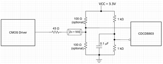
1. How should the circuit of the CLKIN pin be configured when a 3.3V level cmos single-ended signal is used as an input?

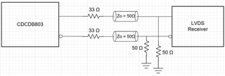
2. How should the circuit of the CK0~CK7 output pins be configured when using the output signals to be compatible with LVDS?

Thanks,

  • Hello,

    1. The CDCDB803 only accepts LP-HCSL inputs. To convert the CMOS signal for a differential input, please use the following termination.

    2. The CDCDB803 only outputs LP-HCSL outputs. To convert the output to LVDS, please use the following termination.

    Regards,

    Kia Rahbar