This thread has been locked.

If you have a related question, please click the "Ask a related question" button in the top right corner. The newly created question will be automatically linked to this question.

LMK04828: Phase fluctuation

Part Number: LMK04828
Other Parts Discussed in Thread: LMK04832, LMK1D1204

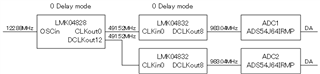
The data acquired by LMK04828 + LMK04832 + ADC (ADS54J64IRMP) are compared.
Even if the SPI is set after the power is turned on and off (the parameters are consistent each time and the parameters are consistent between the two devices), the phase of ADC2 with reference to ADC1 is basically the same phase difference. , There are some fluctuations.
I would like to know if this slight fluctuation is within the permissible range, but how should I consider it? (Jitter?, skew?)

  • Hello user1237122,

    First, effectively all of the variation between the phases of the ADCs will be contributed by skew. The jitter contribution from LMK04828 and LMK04832, when using a clean input reference, is negligible.

    Assuming DCLKout8 is fed back internally as the LMK04832 zero-delay feedback, the zero-delay configuration for LMK04832 guarantees that there will be close phase alignment between the two different devices' DCLKout8 outputs as long as the two 491.52MHz clocks from LMK04828 are also in phase. The only way to guarantee the two 491.52MHz clocks from LMK04828 are in phase is to synchronize the LMK04828, so unless the output clocks are synchronized with the same digital delay programming at some point during the startup and programming of LMK04828 there will likely be significant phase variations between power cycles due to the timing uncertainty setting the channel dividers with SPI programming. 

    Assuming additionally that LMK04828 is synchronized to satisfy the alignment requirement at LMK04832, there are going to be a handful of sources of phase error between the two systems:

    • LMK04828 has some channel-to-channel skew. Using DCLKout0/DCLKout12 from the same clock group helps to minimize this skew, but the value can still be tens of picoseconds. Datasheet provides a typical value of 50ps between any DCLK to any other DCLK, but this could include between clock groups; I expect within the same clock group will be slightly better, maybe 20-30ps range.
    • LMK04832 will have part-to-part variation between CLKout8 phases. These will come from several sources, such as differences in supply voltage, differences in device temperature, and process variation. While you can minimize temperature and voltage variation between different devices, process variation is difficult to control. I don't have an exact magnitude of difference for this variation, but it would not be unreasonable to expect ~50ps between devices due to process variation.
    • The ADC also has some part to part variation. Conveniently this is listed in the datasheet as about ±100ps for devices at the same temperature and supply voltage.

    It seems the magnitude of variation contributed by the clocking devices is substantially smaller than the potential variation between the ADCs. Nevertheless, the skew contribution from clocking devices is non-negligible. I could see a few ways to reduce the skew:

    • Use a buffer with lower channel-to-channel skew, and distribute 122.88MHz to both LMK04832 inputs; then derive 983.04MHz from 122.88MHz. Something like LMK1D1204 specifies a maximum of 20ps channel-to-channel skew, vs unclear but likely 20-30ps range of LMK04828. There may also be some phase noise benefits to this approach, since cascading LMK04828 PLL output into LMK04832 reference will greatly increase the LMK04832's input reference noise vs a clean 122.88MHz source; furthermore, you can double the 122.88MHz in the LMK04832 without losing zero-delay configuration.
    • Keep the LMK04828 and use the analog delays in the DCLKout0/12 outputs to adjust the phase in ~25ps steps if needed. This approach has the advantage of correcting for the entire path's error if needed (including ADC error), but comes at the expense of elevated phase noise from the analog delay circuit.
      • To some extent the elevated phase noise can be mitigated by using the LMK04828 in divide-by-1 distribution mode instead of PLL mode. Lower frequency clocks are typically not be as badly impacted by the analog delay due to the noise floor limitations of the output stages. Of course, in divide-by-1 distribution mode, there will still be phase noise added by the divider and muxes, but it will probably be cleaned up by the LMK04832 loop beyond a few hundred kHz offset. Additionally, there would no longer be a zero-delay relationship between LMK04828 input and output, so if this is relied upon elsewhere in the system you may have trouble.
    • Can the clock fanout be reduced to a single stage, and synchronization can be used to align two outputs of the same clocking device going to different ADCs? This might not work if you're doing some kind of multi-board setup, but it's fewer parts and therefore better worst-case skew.

    Regards,

    Derek Payne