Because of the Thanksgiving holiday in the U.S., TI E2E™ design support forum responses may be delayed from November 25 through December 2. Thank you for your patience.

This thread has been locked.

If you have a related question, please click the "Ask a related question" button in the top right corner. The newly created question will be automatically linked to this question.

TLC551: Oscilation

Part Number: TLC551
Other Parts Discussed in Thread: TLV170

Hi Team,

Can you please check the inquiry below?

A time delay circuit with TLC551CD chip is used in the design with a 2.49Meg in parallel with a 22uF cap connected to the trigger input of the TLC551. The V+ is 12V, THRES connected to GND, CONT & DISCH pins floating. The input to a PMOS on the high side of the res/cap/trigger input that is initially in closed state (so the cap is at 12V), then the input opens the pmos and the res/cap start draining. 

When the trigger input voltage reaches about 4V (where the 551 should trigger the output to change), the device is entering an oscillation where the trigger voltage will go back up to 4.3V, drain back to 4V and repeat endlessly.  The 551 never changes state as a result.  the 12V can be temporarily disabled, allowing the cap to fall down into the 2.5V range, and flip it back on and this will trigger the output to change state and stay there as it should.

Can you please help explain why the trigger input voltage is oscillating with this RC circuit.  Is there some sort of capacitive coupling that is needed to resolve when the output flips?  In monitoring the other pins during the issue, there is no oscillation on V+, Cont, or OUT.  Only the trigger voltage is affected.  The customer verified that none of the other inputs are changing.

Let me know if you need more information.

Regards,

Marvin

  • Marvin, 

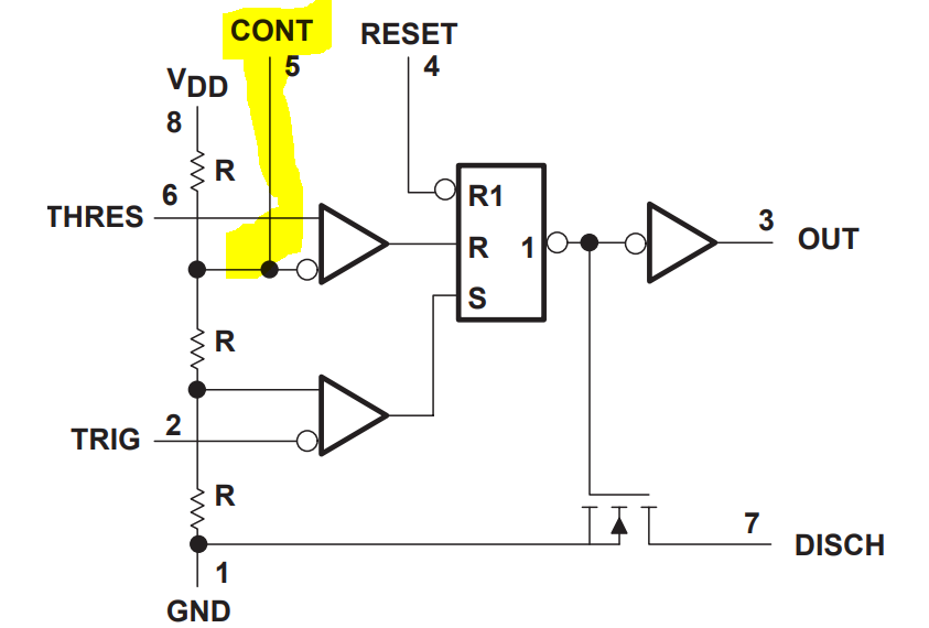
    In the below image you can see that the control pin is attached directly to the top comparator. If the control pin is not being used than we recommend placing a decoupling cap from the control pin to ground. This will help filter out any noise on the comparator input and also help with preventing false tripping. Below you can see that the internal resistor divider results in the 2/3 VDD and 1/3 VDD points for threshold and trigger. I need to think about what happens when the threshold pin is tied to ground in this scenario as this is an uncommon scenario. 

    Has the customer attempted to disconnect the CMOS transistor and check the functionality of the timer isolated in circuit by triggering with a separate supply while monitoring the output? It would help to isolate the issue. 

    Best Regards, 

    Chris Featherstone

  • Hi Chris,

    during the customer probing, they found that the trigger pin was the only one experiencing any oscillation.  The control pin, though it was floating, stayed solid voltage-wise throughout.  So placing a cap across it for filtering would be unnecessary as there wasn't anything to filter.  Would this be okay?

    They haven't attempted to remove the transistor as of yet because the oscillation (a sawtooth waveform fyi) does not start until hitting the trigger point of the 551 chip, so there must be something going on with the 551.  Also (while still monitoring the trigger voltage), when power cycled allowing the RC / trigger voltage to go well below the trigger point and then powering back on, it immediately triggers on the output and the RC voltage continues to drain as you would expect with no more oscillation.

    They have verified this issue on multiple boards (new design), though it still could theoretically be a lot issue with the chips.

    They would try removing the mosfet and If that doesn't work they will attempt to put a schottky diode between the RC circuit and the trigger to prevent whatever leakage current flow that might be coming from the trigger from re-charging the cap. Will this help?

    Regards,

    Marvin

  • Marvin, 

    I am currently looking into this and will need some time for review. I will respond within 2 business days. Thank you for your patience. 

    Best Regards, 

    Chris Featherstone

  • Marvin, 

    Although the filter on the control pin may not be causing this particular issue, we would still recommend that the customer low pass filter this node in the design. This is just a recommendation based on my observations of the schematic. 

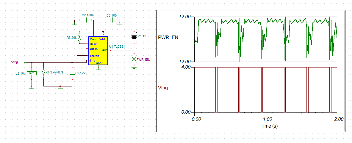
    Regarding the trigger pin oscillation, I am trying to understand the operation of the circuit. I put a subset of the circuit into the Tina Ti simulator. I am using a 4V signal on the trigger pin that would simulate the trigger input signal as described above. The output does not work with this basic setup. The trigger pin is a high input impedance node that is one input of a comparator. There should be no oscillations created by the comparator input. The input current to the comparator is 10 pA typical. There should be no high value leakage current unless the pin is damaged. 

    Is it possible that the TLV170 circuit is oscillating and the oscillation is appearing at the node that the trigger pin is attached to? One other recommendation would be to have an output isolation resistor of the TLV170 to isolate the gate capacitance of the Mosfet. Having a zero ohm placeholder at this node will help in the event that the Op Amp is oscillating. 

    I have attached the simulation. Let me know if you see a mistake in my schematic. I believe this is the general setup simplified however I do not see how this circuit is meant to function yet.

    TLC551.TSC

    Best Regards, 

    Chris Featherstone

  • Hi Chris,

    Thank you for waiting. Here's more information from the customer.

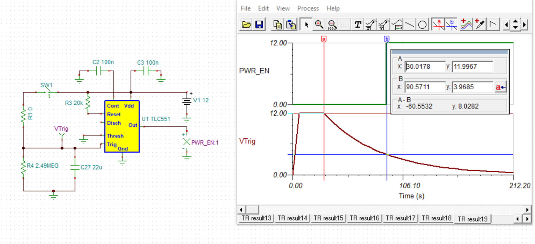
    The circuit is simply a 60sec delay timer to detect an external power-up and provide a delay to a power-up further down the line.  When the external stimulus is off, Vtest is off (0V) going into the opamp, so the fet is on and charging the cap to 12V.  When the external device powers on, a 10V signal is present at the input of the opamp, and it shuts off the FET, starting the 60sec timer.  When the RC circuit reaches approx 4V (1/3 of the 12V input power), the 551 chip toggles the output.  The output in turn turns on 4 separate NMOS fets which apply power to some DC/DC converters and power up the rest of the board.
    The customer builds a partial circuit with only the parts on the image plus a 10k load resistor for testing, With this partial circuit, it all works perfectly with no oscillation.  However when adding the NMOS fets the out pin is controlling, then the trigger line starts oscillating.  The out line is a solid 0V and is not remotely getting close to turning on the NMOS fets to power the DC/DC converter. a DC/DC converter should not make noise if it isn't powered on. Also adding a 1uF cap on the cont pin has no effect.
    what could be the issue source of this issue?
    Regards,
    Marvin
  • Marvin, 

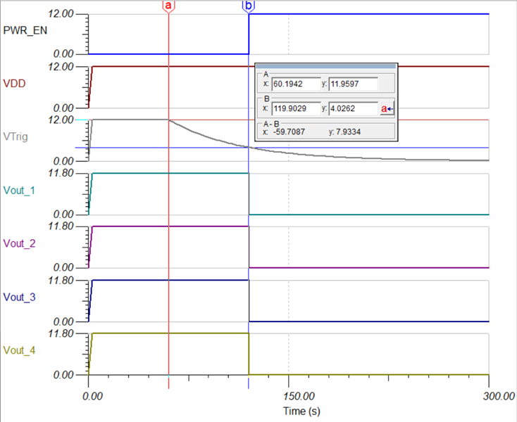
    Thank you for the clarification on how the timer is meant to function in this application. I was able to update my simulation to match the description. See below. I will continue to look into a solution for driving the FETs with the timer output. 

    Best Regards, 

    Chris Featherstone

  • Hello Marvin, 

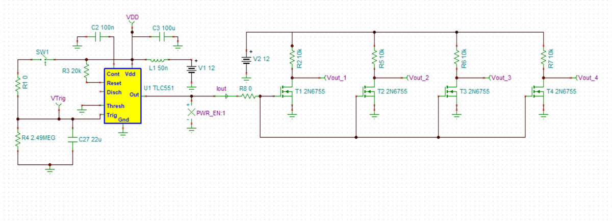
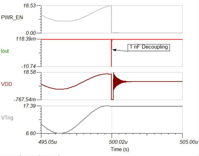
    I suspect that there is a small amount of parasitic inductance on the supply line. Any small amount of parasitic inductance combined with driving large FETs and switching events may be what is causing this issue. I have added the FETs that the 555 timer is driving. In addition I have added 50 nH of supply line parasitic inductance and checked the startup and switching behavior.

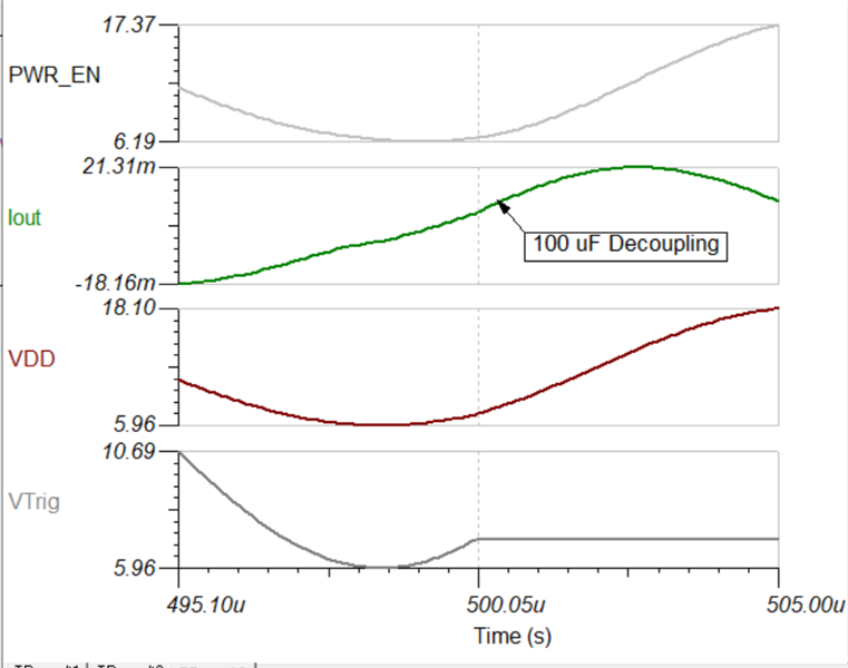
    During the switching event on the trigger line, there is a spike of current as seen on the Iout waveform below. Notice that the value is in the amps range. Any parasitic inductance during these switching events and driving the large FETs will cause a droop in the supply line and can reset the timer and give unexpected results. For demonstration purposes I bumped up the power supply decoupling capacitor to 100 uF to show that the current spike greatly reduces. 

    Notice below that there is a very large surge of current demand and the power supply, VDD droops dramatically. 

    Bumping up the decoupling capacitor value to 100 uF for demonstration shows a significant decrease in the current draw during the trigger switching event. 

    Checking the circuit functionality with the larger decoupling capacitor I see the desired behavior. 

    Here is my Tina simulation:

    TLC551 (1).TSC

    Best Regards, 

    Chris Featherstone