This thread has been locked.

If you have a related question, please click the "Ask a related question" button in the top right corner. The newly created question will be automatically linked to this question.

CDCM61001: Query regarding Pin description. Please see detailed description

Part Number: CDCM61001
Other Parts Discussed in Thread: CDCM9102

1. What is the IO voltage levels for all Pins especially OD, OS, PR pins

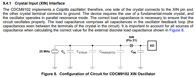
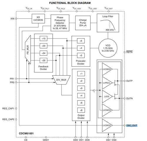
2. In datasheet, only XIN pin is mentioned. Please let me know which is XOUT pin to connect the crystal

3. What is the use of OSC_OUT pin?

4. Can I connect OS, OD and PR pins to VCC or GND instead to operate by GPIO of MCU?

  • Hello,

    Our clock gen experts are out of office today and will be back tomorrow.

    Best,

    Andrea

  • Chintan,

    Please see the levels for the pins here:

    The part uses a Colpitts oscillator circuit as the XTAL input, as is stated here:

    Refer to this excerpt from the CDCM9102 datasheet for the circuit for the XTAL:

    The OSC_OUT pin is a buffered copy of the input clock, as is shown in the functional block diagram:

    The OS*/OD*/PR* pins can be either pulled to VCC/GND through pull-up/pull-down resistors, or can be controlled externally by GPIO. In the latter case, I recommend still using a pull-up/pull-down resistor to set the initial values.
    Thanks,
    Kadeem