A related question is a question created from another question. When the related question is created, it will be automatically linked to the original question.
If you have a related question, please click the "Ask a related question" button in the top right corner. The newly created question will be automatically linked to this question.
Could you please provide the configuration guide for LMX2485E? My client's new project is currently utilizing this component, but we are unaware of how to configure it. Thank you!
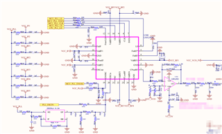
1. I successfully output the data needed to configure the registers using TICS Pro. Currently, the OSC is 19.2Mhz, and I only need to configure the RF high frequency to 650Mhz, the Fpd to be close to 200kHz (bandwidth), and the IF intermediate frequency is not needed. Therefore, the data is as follows:
R0 0xCB0000
R1 0xB0FA03
R2 0x001385
R3 0xFF00A7
R4 0x20C549
R5 0x00000B
R6 0x3C000D
R7 0x00090F
2) To make the LMX2485E work, I pulled LE low, CE high, and ENOSC high. During configuration, the CLK period was approximately 37us. After writing 24 bits of data to the register, I would pull LE high and 17us later pull it low.
Then there are the following questions:
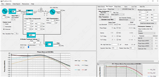
1. I verified that the data and clock signals on the logic analyzer were normal. However, when I looked at the frequency with a spectrum analyzer, it was unchanged, and no matter how long I waited, the LD was not pulled up using a multimeter. Could you please provide a reference for the effective timing of Data and Clock?
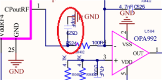
However, once I power up the PLL and VCO, the CpoutRF will soon drop to 0V, so as the output of the loop filter. The output of the loop filter also rise to 13V after it stay 0V for few seconds.
My start up sequence is CLK, Data, CE, ENOSC set HI, LE set LOW, after around 5ms, I start to write register values. I set LE HI for 18us then set it LOW for each address.