Tool/software:
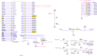
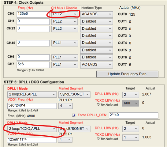
On the circuit, the 'LMK05028' and the oscillators (XO, TCXO) mentioned below are installed. Ref_IN1 is fed with 5MHz (LVCMOS). We want to synchronize 125MHz (Out0) with REF_IN1.
Several tests were done by different threshold and LBW values and afterwards we looped back (5MHz) Out7 to REF_IN1, but DPLL1/2 did not lock.
Test conditions:
TICS file:
LMK05028_SyncE.tcs
XO Oscillator: 48MHz ±50ppm (ECS-3225MV-480-BN)
TCXO Oscillator: 19.2MHz ±1ppm (525L19210IT)
By programming the board with “LMK05028_SyncE.tcs” XO، TCXO and REF_IN1 deliver no fault.
Read Reg 0x0D = 0x00 (XO and TCXO Validated)
Read Reg 0x2E6 = 0x20 (REF_IN1 Validated)
REF_IN1 Monitor mask register is as below:
Write Reg 0xBE = 0x2F
Although APLL is locked, DPLL1/2 frequency and phases are not locked.
Read Reg 0x0D = 0x00 (APLL 1/2 Locked)
Read Reg 0x0E = 0xC0 (DPLL 1 Not Locked)
Read Reg 0x0F = 0xC0 (DPLL 2 Not Locked)
My Schematic:LMK05028_SyncE.TCS