Tool/software:
By reading datasheet it is not really clear on
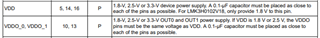
- can i use different voltages on VDDO_0 and VDDO_1 ?
For example, when VDD is 3.3V, can i use VDDO_0 as 1.8V and VDDO_1 as 3.3V ?
OUT0 and OUT1 intended to be LVCMOS 25 MHz outputs
- what is the REF_CLK output VDDO voltage ?
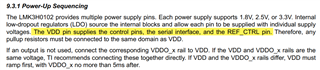
In table 5.5, LVCMOS REFCLK CHARACTERISTICS test conditions speak about VDDO 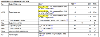
and in chapter 9.3.1 says REF_CTRL (same pin) is supplied from VDD