CDCE6214: Logic Compatibility Check: CDCLVC1310RHBR (1.8V) to CDCE6214RGET (1.8V)

Part Number: CDCE6214
Other Parts Discussed in Thread: LMK3H2104

Tool/software:

We are planning to use CDCLVC1310RHBR as the input source to CDCE6214RGET (configured for PCIe clock generation). Both devices are powered at 1.8V

Can you please confirm:

  1. Is it safe to connect CDCLVC1310RHBR output directly to CDCE6214RGET input at 1.8V?
  2. Are there any known issues or recommendations for this configuration?

Thanks,

Pradeepraj M

  • Pradeepraj,

    No issue that we are aware of. Please note this information from the datasheet for providing a single-ended input to the CDCE6214:

    Thanks,

    Kadeem

  • Upon checking the datasheets, we observed a logic compatibility issue:

    • CDCLVC1310RHBR:
      • VOH (min): 1.26V
      • VOL (max): 0.44V
    • CDCE6214RGET:
      • VIH (min): 1.44V
      • VIL (max): 0.36V

    This results in:

    • VOH1 (min) > VIH2 (min) → Fails
    • VOL1 (max) < VIL2 (max) → Fails

    Could you please confirm.

  • Pradeepraj,

    This understanding is correct. If the high level voltage of the buffer is lower than the minimum high level of the clock generator, then there is risk of the clock generator not operating properly. The same is true for the low level behavior.

    What is driving the input clock of the buffer? We may have alternative solutions for the system that we can recommend. LMK3H2104 may be used to replace the LVCMOS buffer and its input.

    Thanks,

    Kadeem

  • Hi Kadeem,

    We are using the CDCE6214RGET in our design with the HW_SW_CTRL pin tied low, which means the device operates in Pin Mode and loads EEPROM Page 0 at power-up. The I²C interface is not connected in our schematic.

    We would like to configure:

    • OUT1 as LP-HCSL
    • OUT4 as LVDS-like

    Could you please clarify the following:

    1. What is the default output logic type for each channel when HW_SW_CTRL is low and the device loads EEPROM Page 0?
    2. Is it possible to configure OUT1 as LP-HCSL and OUT4 as LVDS-like using only hardware strapping or termination, without enabling I²C or modifying EEPROM content?
    3. If not, what is the recommended method to achieve this configuration in Pin Mode?
    4. Are there any specific termination or layout guidelines when mixing LP-HCSL and LVDS outputs across different channels?
  • Pradeepraj,

    The default is LP-HCSL for all differential outputs.

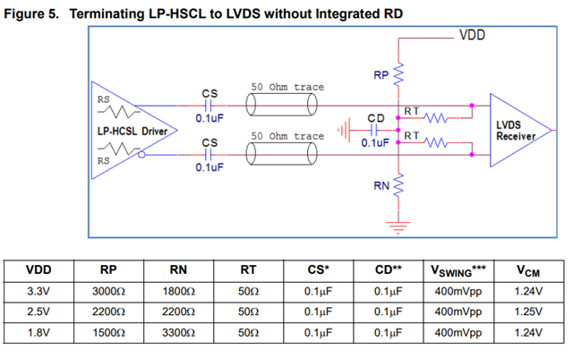
    The closest that you can get to LVDS from LP-HCSL is to AC-couple the LP-HCSL output, and connect as such:

    AC-couple the clocks close to the driver, and place the termination resistors close to the LVDS receiver.

    Thanks,

    Kadeem

  • Hi Kadeem,

    LVDS receiver is ArtiX 7 FPGA (XC7A100T), Currently we are using AMD recommended termination for LVDS to HCSL. I attacjhed the reference below. Kindly confirm is it valid to use in design and share the document link you gave above for clock termination.


    Thanks,

    Pradeepraj

  • Pradeepraj,

    The clock termination document that I was referring to can be found here: https://www.renesas.com/en/document/apn/891-driving-lvpecl-lvds-cml-and-sstl-logic-universal-low-power-hcsl-outputs.

    The termination is integrated, so the series 33 Ohm resistor is not necessary.

    Thanks,

    Kadeem