This thread has been locked.

If you have a related question, please click the "Ask a related question" button in the top right corner. The newly created question will be automatically linked to this question.

problems of LMK04816

Other Parts Discussed in Thread: LMK04816, CODELOADER

SIR:

I use LMK04816 in my design for the first time in my design. I encounter some problems that is puzzled me.

I reset the device through the configure of register R0, then I configure register R0 to R31 according to my design. After that, clockout0, clockout2, clockout6, clockout8, clockout10 produce output clock in 250Mhz, which is coincident with my design. But:

  1. I configure LD_MUX R[31:27]= 3, which means Status_LD pin is connected to “PLL1 & PLL2 DLD”. I configure LD_TYPE R[26:24]=3, which means the Status_LD pin is Output(push-pull).

    But the Status_LD pin is not active. What is the possible reason for this problem?

  2. When I test the output clock using oscilloscope, I find the 5 output clocks are not in the same level standard. In fact, I configure all the 5 clocks in the same level standard(1600mV LVPECL). Like, the peek-to-peek value for one signal of the differential of clockout2 and clockout6 is about 500mV, while the peek-to-peek value for clockout8 and clock10 is about 900mV. But for clockout0, one signal of the differential clock has a peek-to-peek value of about 900mV, the other has a value of 160mV. What’s the possible reason for this problem?


    Regards

    Thanks

    Jacky

    2014-01-18

  • By the way, I configure the LMK04816 as follow:

  • Can some body give me some suggestion?

    Thanks

    Regards

  • Hi Jacky,

    Are you testing this on the LMK04816 evaluation board from TI, or on your application board?  If it's your application board, could you please send your LMK04816 schematic?

    Also, could you please send the CodeLoader setup file (.mac file) used to program the device registers?

    Do you see Status_LD pin is asserted if you set LD_MUX = "PLL2 DLD"?  How about if LD_MUX = "PLL1 DLD"?  If either of these PLL are not locked, then "PLL1 & PLL2 DLD" will not be asserted.

    Regarding your other question, did you check the output load termination on the board matches the programmed LVPECL 1600 mVpp output format?  This is one explaination for why the output swing is different.

    Regards,
    Alan


  • Alan:

    Thank you for your kindness!

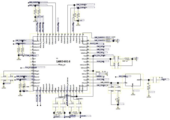
    (1) I am doing the test on my own application board, and the LMK04816 schematic is showed below.

    (2) Sorry, I do not use the Codeloader. I use the FPGA on my board to configure LMK04816, and I  generate the Register map value by careful calculating. I also paste the register map value below.

    (3) Besides the configuration of LD_MUX=PLL1 & PLL2 DLD, I also set LD_MUX=PLL1 DLD, but the STATUS_LD pin is not asserted either.

    (4) Because I use the LVPECL standard for the output clock, each of the differential pin is terminated to GND through a 240ohm resister. I check the output load, and all the load are 240ohm.

    Appendix 1: schematic of LMK048616

    Appendix 2: the Register map for LMK04816 in verilog

     always@(negedge CLK_LMK)
     begin
      case(CNT2)
      6'b000000: LMK_REG_TEMP<={32'b0000_0000000000_1_0_00000000000_00000};//R0 for reset;
      6'b000001: LMK_REG_TEMP<={32'b0000_0000001101_0_1_00000001010_00000};//config R0;
      6'b000010: LMK_REG_TEMP<={32'b0000_0000001010_0_0_00000001010_00001};//config R1;
      6'b000011: LMK_REG_TEMP<={32'b1000_0000000000_0_0_00000000000_00010};//config R2;
      6'b000100: LMK_REG_TEMP<={32'b0000_0000000101_0_0_00000001010_00011};//config R3;
      6'b000101: LMK_REG_TEMP<={32'b0000_0000001000_0_1_00000001010_00100};//config R4;
      6'b000110: LMK_REG_TEMP<={32'b0000_0000000101_0_0_00000001010_00101};//config R5;
      6'b000111: LMK_REG_TEMP<={32'b0000_0100_0000_0100_00000_0_00000_00110};//config R6;
      6'b001000: LMK_REG_TEMP<={32'b0000_0100_0000_0000_00000_0_00000_00111};//config R7;
      
      6'b001001: LMK_REG_TEMP<={32'b0000_0100_0000_0100_00000_0_00000_01000};//config R8;
      6'b001010: LMK_REG_TEMP<={32'b0001_0000_0_0_0_0_0_000_010_0_0_010_000_01010};//config R10;
      6'b001011: LMK_REG_TEMP<={32'b00000_1_1_1_0_0_0_0_00_0_1_0_001_000000_0_01011};//config R11;
      6'b001100: LMK_REG_TEMP<={32'b00011_011_0_0_0011000000000_1_01_1_01100};//config R12;
      6'b001101: LMK_REG_TEMP<={32'b00111_011_0_000_0_010_1_000_011_0_1_1_1_01101};//config R13; 
      6'b001110: LMK_REG_TEMP<={32'b11_0_1_0_010_0_0_0_0_000000_00_000000_0_01110};//config R14;
      6'b001111: LMK_REG_TEMP<={32'b1000000000_0_0_00001000000000_0_01111};//config R15;
      6'b010000: LMK_REG_TEMP<={32'b00_000001_01010101_00000100_000_10000};//config R16;
      
      6'b010001: LMK_REG_TEMP<={32'b0000_0000_0_000_0_000_0_000_0_000_11_0_11000};//config R24;
      6'b010010: LMK_REG_TEMP<={32'b0000000100_00_00010000000000_0_11001};//config R25;
      6'b010011: LMK_REG_TEMP<={32'b00_0_0_11_111010_10000000000000_0_11010};//config R26;
      6'b010100: LMK_REG_TEMP<={32'b000_1_11_00_00_00_00000000000011_0_11011};//config R27;
      6'b010101: LMK_REG_TEMP<={32'b000000000001_00000000000011_0_11100};//config R28;
      6'b010110: LMK_REG_TEMP<={32'b00000_001_0_000000000000000101_11101};//config R29;
      6'b010111: LMK_REG_TEMP<={32'b00000_101_0_000000000000000101_11110};//config R30;
      6'b011000: LMK_REG_TEMP<={32'b0000000000_0_11111_0000000000_0_11111};//config R31;
      

      default: LMK_REG_TEMP<=32'h0000_0000;
      endcase

    Thanks

    Regards

    Jacky

    2014-01-22

  • Hi Jacky,

    The PLL1 loop filter values in the schematic do not seem to match the values in the simulation.  For PLL1, what is the value of R2?  I could not read the R2 value in the schematic due to the image resolution.

    Also, what is the VCXO's Kv value (in kHz/V)?

    Here are some PLL troubleshooting tips:

    To confirm PLL1 operation/locking:

    1) Program LD_MUX = “PLL1_R/2”

    2) Confirm that LD pin output is half the expected phase detector frequency of PLL1.

    i. If not, examine CLKin_SEL programming.

    ii. If not, examine CLKin0_BUFTYPE / CLKin1_BUFTYPE.

    iii. If not, examine PLL1 register R programming.

    iv. If not, examine physical CLKin input.

    3) Program LD_MUX = “PLL1_N /2”

    4) Confirm that LD pin output is half the expected phase detector frequency of PLL1.

    i. If not, examine PLL1 register N programming.

    ii. If not, examine physical OSCin input.

    Naturally, the output frequency of the above two items, PLL 1 R Divider/2 and PLL 1 N Divider/2, on LD pin should be the same frequency.

    5) Program LD_MUX = “PLL1_DLD”

    6) Confirm the LD pin output is high.

    i. If high, then PLL1 is locked, continue to PLL2 operation/locking.

    7) If LD pin output is low, but the frequencies are the same, it is possible that excessive leakage on Vtune pin is causing the digital lock detect to not activate. By default PLL2 waits for the digital lock detect to go high before allowing PLL2 and the integrated VCO to lock. Different VCXO models have different input leakage specifications. High leakage, low PLL1 phase detector frequencies, and low PLL1 charge pump current settings can cause the PLL1 charge pump to operate longer than the digital lock detect timeout which allows the device to lock, but prevents the digital lock detect from activating.

    i. Redesign PLL1 loop filter with higher phase detector frequency

    ii. Redesign PLL1 loop filter with higher charge pump current

    iii. Isolate VCXO tuning input from PLL1 charge pump with an op amp.

    To confirm PLL2 operation/locking:

    1) Program LD_MUX = “PLL2_R/2”

    2) Confirm that LD pin output is half the expected phase detector frequency of PLL2.

    i. If not, examine PLL2_R programming.

    ii. If not, examine physical OSCin input.

    3) Program LD_MUX = “PLL2_N/2”

    4) Confirm that LD pin output is half the expected phase detector frequency of PLL2.

    i. If not, confirm OSCin_FREQ is programmed to OSCin frequency.

    ii. If not, examine PLL2_N programming.

    Naturally, the output frequency of the above two items should be the same frequency.

    5) Program LD_MUX = “PLL2 DLD”

    6) Confirm the LD pin output is high.

    7) Program LD_MUX = “PLL1 & PLL2 DLD”

    8) Confirm the LD pin output is high.


    Regards,
    Alan

  • Alan:

    Thank you for your suggestions. I will check the them one by one carefully.

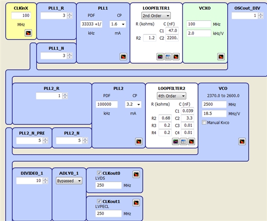
    For  loop filter of PLL1, C1=47nF, R2=1200ohm, C2=2200nF, and the configuration picture(getted from Clock Design Tool) is showed below.

    For VCXO, I use CVHD-950 100.00MHz. The tuning sensitivity is +25ppm/V typical, which is about 2.5KHz/V.

    Thanks

    Regards

    Jacky

    2014-01-22

  • Hi Jacky,

    In addition to trying the debug steps I outlined previously:

    It is possible for the VCXO input impedance to be low enough to cause leakage on the PLL1 charge pump/loop filter node, which causes the PFD reference input and feedback input edges to have some phase offset, even though the PLL is locked and operating stable.  In this case, programming the the PLL1 Digital Lock Detect (DLD) window size register setting to be greater than the phase offset at the PFD input can fix the PLL1 DLD status issue.

    For now, I will close this thread.  If you haven't resolved the issue after trying all the debug suggestions, you can reply to (re-open) the thread and we can resume troubleshooting.

    Regards,
    Alan