This thread has been locked.

If you have a related question, please click the "Ask a related question" button in the top right corner. The newly created question will be automatically linked to this question.

CDCLVP1102: CDCLVP1102 does not have the output signal

Part Number: CDCLVP1102
Other Parts Discussed in Thread: CDCLVP2102, CDCLVP1204, CDCVF2505

Hi team,

The customer is using CDCLVP1102. He uses the single-ended input. He tests the Vac_ref pin and it has a 2V voltage.

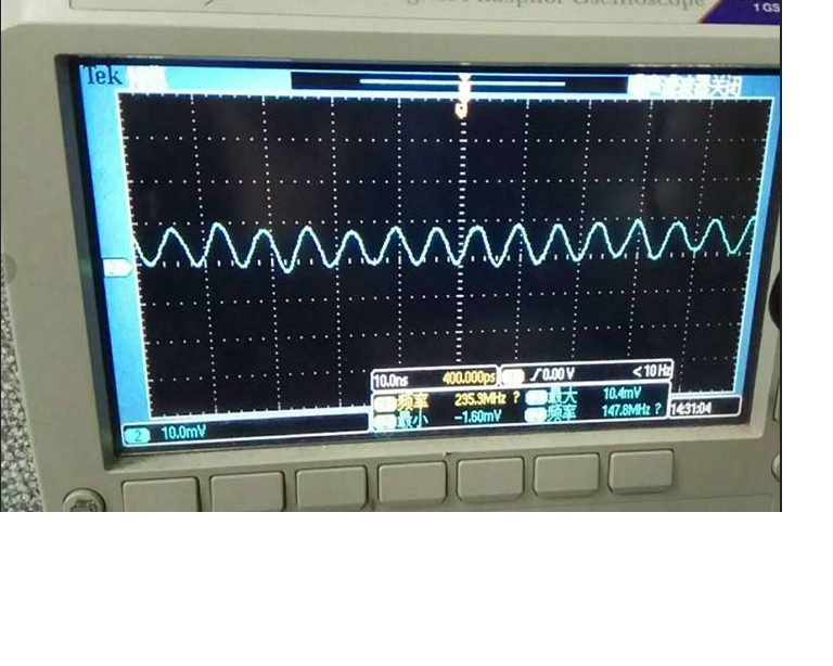
The schematic is in the attachment. When he uses 148.5MHZ or 200MHZ as the input clock frequency,but there is no output signal waveform in

the oscilloscope.He uses LVPECL to output.

Would you provide some suggestions for the customer's issue? Is his schematic correct?

Best Wishes,
Mickey Zhang
Asia Customer Support Center
Texas Instruments

  • Hi Mickey,

    The schematic looks fine. 2V Vac_ref is also within spec.

    Can you check the LVPECL output termination? There do not appear to be resistors to GND. Follow the example in section 8.4.1 of the datasheet, 'LVPECL Output Termination' (also shown below):

    Regards,

    -Tim

  • Hi Tim,

    I have confirmed with the customer.

    The customer's schematic is the AC coupling. Actually, the customer uses DC coupling on his board through the fly

    lines. He refers to the (a) Output DC Termination of Figure 13. But he uses 180 ohm and 110 ohm to replace 130 ohm

    and 82 ohm for the (a) Output DC Termination.

    Finally, there is no output waveform in the oscilloscope.

  • Hi Mickey,

    Can you verify the high and low voltage of the LVCMOS input and verify that 2V (coming from Vac_ref) is roughly the average? Refer to figure 14 of the datasheet for proper single ended input biasing.

    Regards,

    -Tim

  • Hi Tim,

    The customer has verified the information. It is as below:

    VIH=1.4V, VIL=1.2V. Vac_ref=2V, The 2V of Vac_ref value remains the same.

    For the figure 14 of the datasheet, how to calculate the RS value?

    If the RS value is incorrect, does this value cause no output signal?
  • Hi Mickey,

    The voltage into the INN pin needs to be the average of the Vih and Vil levels. Since in this case it is set to 2V by Vac_ref, but both Vih and Vil are lower than that, the device thinks the clock is always low. In this case, the customer needs INN to be biased to 1.3V using resistor dividers (value not important, higher values consume less current), so Vac_ref cannot be used. Refer to figure 3 of the datasheet (below):

    Additionally, the input swing the customer is using is not large enough- the datasheet states that the minimum swing must be Vth+/-0.1V. With a swing of 0.2V this case is marginal if Vth is perfectly centered at the average, but since in actual use it will not be perfectly centered, so the input will not meet the required spec.

    Regards,

    -Tim

  • Hi Tim,

    Thanks for your help.

    Q1: You mean the Vac_ref pin can be floating and add a 1.3V bias voltage to INN pin,

    then the issue will be solved, right? Does Vac_ref pin still need a 0.1uF capacitance like the customer's schematic?

    Q2:  The VIH 1.4V is higher than Vth 1.3V. The VIL 1.2V is less than Vth 1.3V. 

    What do you mean by "With a swing of 0.2V this case is marginal if Vth is perfectly centered at the average, but since in actual use it will not be perfectly centered, so the input will not meet the required spec"? Would you explain more about this?

    Does you mean the VIH 1.4V and VIL  1.2V cannot meet the input level voltage range? What is 0.2V you said?

  • Hi Mickey,

    1. Correct, Vac_ref can be left floating. This should solve the issue but I still have concerns over the signal swing (see #2):

    2. In the datasheet, the min spec is that Vih needs to be 0.1V above Vth, and Vil needs to be 0.1V below Vth. If they are using a signal with Vih and Vil exactly +/-0.1V I am concerned that it will not meet the spec- they should ideally make the swing larger to build in some margin to account for variation.

    Regards,

    -Tim

  • Hi Tim,

    Q1: Now the customer add a 1.3V bias voltage to INN pin, and the Vac_ref pin is connected

    a 0.1uf capacitance to GND like the customer's above schematic. then CDCLVP1102 can

    output the clock signal.

    You mean the Vac_ref pin can be floating and the 0.1uF capacitance can be removed, right?

    Q2: The customer also would like to know what are the differences between CDCLVP1102, CDCLVP2102 and

    CDCLVP1204? For the customer's application, if the input frequency is the same,

    can the schematic for these three devices be the same?

    Q3: The customer would like to use CDCVF2505+CDCLVP1102 for their application.

    The input frequency 148.5MHZ is input to CDCVF2505, then the output frequency of CDCVF2505

    is connected to the input channel of CDCLVP1102. When the customer tests CDCVF2505 alone,

    the output frequency is the same as the input frequency. But the amplitude of the output signal is

    reduced. When the 148.5MHZ is input to CDCVF2505, then CDCLVP1102 cannot output the clock signal.

    For this issue, would you provide some suggestions?

    Would you provide a reference schematic for CDCVF2505?

    For the CLKOUT pin, how to deal with it? connect a 0.1uF capacitance to GND? Or floating?

    For the 1Y0~1Y3 pins, if there is a unused pin, can it be floating?
  • Hi Tim,

    Would you continue to support the customer's issue?
  • Hi Mickey,

    1. Yes, Vac_ref can be left floating if unused.

    2. The difference between these parts is as follows. See also the block diagram in the respective datasheets.
    CDCLVP1102: 1:2 LVPECL buffer
    CDCLVP2102: 2x 1:2 LVPECL buffer (it is like having 2 CDCLVP1102 in the same package)
    CDCLVP1204: 4 output LVPECL buffer with 2 inputs connected to a mux

    The configuration for each of these devices is the same so the schematic can be reused- the only difference being the number of inputs/outputs and the addition of an input select for the CDCLVP1204.

    3. Can you probe the clock signal at the INP pin of CDCLVP1102 with a high impedance probe? Ensure that the voltage bias Vth at INN is halfway between Vih and Vil. Also, ensure that Vih is greater than 0.1V above Vth and greater than 0.1V below Vil.

    Unfortunately there are no reference schematics available but you can refer to the Application and Implementation section of the device datasheets.

    CLKOUT and unused outputs on the CDCVF2505 can be left floating if unused.

    Regards,

    -Tim

  • Hi Tim,

    The customer has verified.

    The input clock frequency is 148.MHZ and it is about 50mV for the INP pin. 

    Since the output voltage is very small, he cannot verify the Vth VIH and VIL.

    The CDCVF2505 schematic is in the attachment. 

    Is the schematic correct?

    For the customer's description, when the customer tests CDCVF2505 alone, the output frequency is the same as the input frequency.

    But the amplitude of the output signal is reduced.

    Why will the output amplitude be reduced? Is is possible the CDCVF2505 device is bad? 

  • Hi Mickey,

    Yes, a swing of 50mVpp is too small for the CDCLVP1102.

    Looking at the schematic, the 22pF capacitor and 500ohm resistor are not necessary (In the datasheet, they are used as a test load). Try removing them and see if the output amplitude increases.

    Regards,
    -Tim
  • i Tim,

    When the customer remove the 22pF capacitor and 500ohm resistor, the output amplitude is is almost unchanged. 

    Please check the attachment. The first screenshot is the keeping the 22pF capacitor and 500ohm resistor screenshot.

    The second  screenshot is the removing the 22pF capacitor and 500ohm resistor screenshot. 

    Do you have any other suggestions?

  • Hi Tim,

    Would you continue to provide some suggestions?
  • Hi Mickey,

    When they measure the waveform above, is the CDCVF2505 connected to the CDCLVP1102?

    Could you share the schematic showing the connection from CDCVF2505 to CDCLVP1102?

    Regards,
    -Tim