Other Parts Discussed in Thread: LMK04828
Hi,
I wonder if you can help me please?
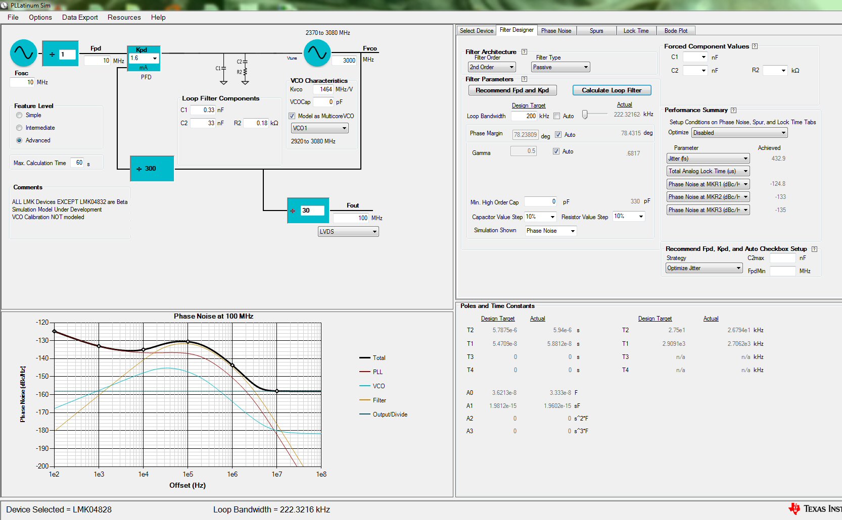
I have inherited a project from a colleague who has now left and am trying to see if the design is reasonable. Essentially he used a LMK04828BISQ (Clock Jitter Cleaner with Dual Loop PLLs) to produce a series of 100 MHz and 200 MHz clocks from a 10 MHz LVDS TCXO. However, he only used half the chip and fed the TCXO into pins 43 / 44 (OSC in) thus bypassing the first PLL. I have 3 questions:-
1). When using a TCXO rather than degraded clocks that have travelled some distance is it reasonable to use the chip in this manner or will it degrade the jitter performance?
2). Would it make more sense and produce less jitter if the TCXO was say 50 or 100 MHz?
3). I have tried to use the TI Clock Design Tool version 1.3.5 to check the loop filter design. However it doesn’t appear to support the mode I am forced to use as it immediately starts to use both PLL sections. Is there a work around for this please? Also in the select solution part of the program there are 2 options for the LMK04828B VCO0 and VCO1, what is the difference between them?
Many thanks for your help
Best regards
Keith