Other Parts Discussed in Thread: LMK04828, ,
Demand:
The modulation and demodulation board mainly uses BPSK signal to achieve high-precision ranging. The chip rate of the signal is 100MHz, the occupied bandwidth is 200MHz, and the carrier frequency is 1.2Ghz. It is required that each power on reference clock should be consistent with the phase of each part of the system, and have repeatability, that is, there is a deterministic phase relationship. The frequency of external reference signal is 100MHz, which is the signal after frequency doubling of hydrogen atomic clock. The stability and phase noise are very good. Therefore, when choosing the clock chip, do not choose the double loop PLL with external crystal oscillator. The clock chip will deteriorate the input reference signal index (such as 7044).
The sampling rate of dac9172 is 9.6GHz and BPSK carrier is 1.2Ghz. The two baseband data rates (I-channel data and Q-channel data) provided by FPGA to DAC are greater than 300MHz and integral multiples of 100MHz respectively.
The sampling rate of ADC of receiving board is about 3GHz (to be determined). At present, ad9208 is tentatively determined, and BPSK carrier is 1.2Ghz. The sampling rate output to FPGA after decimation is about prime frequency within 300MHz ~ 500MHz (for example, 499.99mhz, 333.49mhz).
Plan:
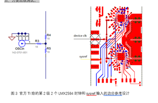
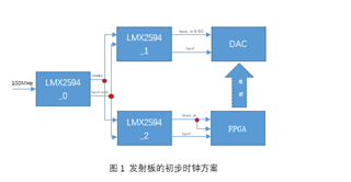
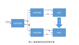
At present, the possible clock scheme is to use three lmx2594 chips to realize the system. This scheme is officially given by Ti (the information name is "phase synchronization reference design of multiple PLL synthesizers", which I have published in the group). In the reference design, the clock input and sysref synchronization pulse of two lmx2594 chips in the second stage are required to be provided for the same clock chip, so as to realize the system The input and output clocks of two lmx2594 chips have deterministic phase. For this kind of application, it is officially recommended to use lmx2594evm or lmk04828evm to provide this clock and sysref, but the phase noise deteriorates seriously when lmk04828 generates prime frequency, so lmx2594evm can be selected as the first stage clock chip, as shown in Figure 1 and Figure 2.
For our application, if lmx2594 works in Category3 mode, that is, there is no integer multiple relationship between lmx2594 input 100MHz and output, then lmx2594_ 1/ LMX2594_ 2 requires lmx2594_ 0 provides strict clock and synchronization signal, which is used to determine the phase relationship between the input and output of the second stage lmx2594, lmx2594_ 0 provides the clock and synchronization signal and needs phase alignment.
Note: when the lmx2594 works in the mode of category1 and category2, the input reference frequency range is 0 ~ 1400mhz if the two lmx2594 of the second stage are synchronized; when the lmx2594 works in the mode of Category3, the input reference frequency range is 0 ~ 100MHz if the two lmx2594 of the second stage are synchronized; (the P11 table and figure 27 of the lmx2594 chip manual can be found.)
Existing problems
At present, the crux of the problem lies in whether the position of the red dot in Figure 1 and Figure 2 is allocated by direct work sharing or by using the clock buffer with fixed delay. The official evaluation board uses direct power sharing method to evaluate lmx2594 at the two red dots on the left_ The output clock of 0 and sysref are allocated, and the synchronization is achieved by controlling the line length, as shown in Figure 3. If buffer is used, the jitter introduced by buffer should be less than 1ps (many are about 100fs). At present, which method we use needs to be further determined. It's better to find ti's engineers to determine. At present, can we design redundancy through buffer or power sharing? It is better to set test points for each node of the clock link to facilitate subsequent testing.