This thread has been locked.

If you have a related question, please click the "Ask a related question" button in the top right corner. The newly created question will be automatically linked to this question.

clock input buffer voltage level for C6678

Other Parts Discussed in Thread: CDCE62005

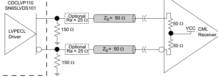
I was really confused about the voltage level about C6678`s clock input. C6678 ` s data manual tells us that LJCB is ranged from -0.3V to 1.3V in table 6-1.but when I was reading "Clocking Design Guide for KeyStone Devices"--SPRABI4—November 2010, I can`t find the threshold limits about the LJCB in table 1, then I checked the whole table , I thought only HSTL standards could meet the requirements(-0.3 to 1.3V), because even the LVDS(1.8V) need 1.8V to identify VIH(min). Then In the EVM ,the chip CDCE62005 provide LVPECL/LVCMOS/LVDS output voltage level ,but does this meet the LJCB voltage range?

thanks!

  • Hi Philly,

    Please see Page 23 of the document at the link below. It shows how to interface an LVPECL clock output to a LCJB Input on the DSP

    http://www.ti.com/lit/an/sprabi4/sprabi4.pdf

    Regards

    Arvind Sridhar

  • Hi Philly,

    additional to the reply to Arvind:

    Please have a look in the "Hardware Design Guide for Keystone1" http://www.ti.com/lit/an/sprabi2c/sprabi2c.pdf

    <Quote> "All clock inputs are differential and must be driven by one of the specified differential
    driver types. All differential clock inputs are implemented with Texas Instruments low
    jitter clock buffers (LJCBs). These input buffers include a 100-ohm parallel termination
    (P to N) and common mode biasing. Because the common mode biasing is included,
    the clock source must be AC coupled. Low voltage differential swing LVDS and
    LVPECL clock sources are compatible with the LJCBs." <unQuote>

    The AC-coupled LVDS/LVPECL outputs of CDCE62005 are compatible with the LJCB.

    Best regards,

    Julian

  • Hi Julian,

    thanks for the answers.

    Still, I want to kown if  CDCE62005s are configured to LVPECL or LVDS modes in the EVM .because I followed the words bellow:

    <Quote>"For additional information on AC termination
    schemes, see the AC-Coupling Between Differential LVPECL, LVDS, and CML
    Application Report (SCAA059).Note that the LJCB clock input is assumed to be a CML
    input in this document."<unQuote>

    There are difference between LVPECL and LVDS. It shows:

    but it likes none mode above from the CDCE62005 drive end to C6678 receive end. Did I missed some point again?

    regards.

    Philly

  • Hello Philly,

    the LVPECL termination is correct. the LVDS termination does not need the 10k pullup/down as the CML receiver has internal biasing.

    On the C6678 EVM the CDCE62005 is configured to LVDS. In the schematic you can see the LVDS termination (only AC coupling caps needed).

    at this page you will find the links to all schematics etc:

    http://www.ti.com/tool/tmdsevm6678

    Best regards,

    Julian

  • Hello Arvind,

    Thanks for the answers.

    Best Regards.

    Philly

  • Hi Julian,

    Thanks a lot.Finally,I think I got it.

    Best Regards,

    Philly