This thread has been locked.

If you have a related question, please click the "Ask a related question" button in the top right corner. The newly created question will be automatically linked to this question.

ADS1282EVM-PDK: ADS1282EVM-PDK

Part Number: ADS1282EVM-PDK
Other Parts Discussed in Thread: ADS1282, ADCPRO, ADS1261, OPA1632, ADS1262, REF70

Hi,

We bought a ADS1282 EVM PDK kit. Kit is working fine.We are using adc pro software for configuring and analysing ADS1282 EVM PDK kit.
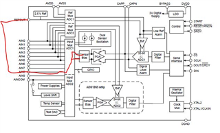
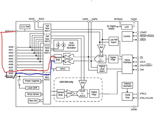
We are applying 10mV input to channel 1 of ADS1282 with following configuration sinc+lpf filter selection, 250sps,pga=1,chop ON the counts come around the
calculated value(Counts varying from 4337187 to 4351272). But when i use same configuration with sinc+lpf+hpf filter selection the count is wrong
(Counts varying from -6464 to 7745). We need a speedy solution to our problem .

Regards,

Venkatavel

  • Hi Venkatavel,

    When you enable the HPF on the ADS1282 it will significantly attenuate any DC signals provided to the input, leaving only the AC noise shown in the output codes.

    I tried applying a 2V dc signal to the ADS1282 and enabling the HPF and I observed the average code change from 852484280 codes (with the SINC + LPF) to 12 codes (with the SINC + LPF + HPF).

    If we're to instead apply a 10mV ac signal (between 25 and 100 Hz) then you should be able to look at the RMS value and still see this AC signal when using the HPF.

    NOTE: In ADCPro the RMS value is shown in the "MultiHistogram" tool and is labelled "StDev" in the DC Analysis display.


    Let us know if that resolves the issue!

    Best regards,
    Chris

  • Hi Chris,
    Thank you for your reply.Our application is DC mV(Upto 80mV).We require noise free 800,000 counts for 80mV input at pga=16 and Vref=5V.
    Can you suggest the best configuration to achieve this count.

    Regards,
    Venkatavel.

  • Hello Venkatavel,

    Short Summary:

    In general, there are a lot of caveats needed to get the performance you’re looking for with the ADS1282. ADS1261 might be a better part for you because the DC performance is a better than the ADS1282.

    But if you’d like to use the ADS1282, the best config will be a gain of 16 or 32 at 250 SPS, where you’ll need to take a 7-sample average to obtain the 800k noise free counts (which is 100nVpp noise resolution). Taking a look at the ADS1261, you can obtain that resolution with many gain settings below 16.6 SPS (and quite a bit less cost).

    Note, the OPA1632 on the ADS1282 EVMs have a lot of 1/f flicker noise that will interfere with your measurement so you would have to take even more samples to ensure noise isn’t affecting the measurement.

    Longer Summary:

    So, I’ll derive the use for the settings here, otherwise, the short summary already has the config you need.

    Resolution we needed

    800k noise free samples with a 80mV range works out to:

    80mV/800k = 100 nVpp


    Getting noise of ADC from SNR to Vpp:

    • You can find the SNR vs data rate table in the datasheet

    • Getting from SNR to input-referred RMS noise is given in the datasheet as well.

    • Which then you can derive the input referred noise in RMS

    As you can see, the lowest is 250 SPS with gain = 16 or 32. However this is RMS noise and we need peak to peak noise.

    • Between the TIPL Statistics Behind Error Analysis of ADC System and understanding of the Crest factor (which is the ratio between peak amplitude and divided by RMS) we can simply multiply the RMS by the crest factor to get a peak to peak value. Experience says, 4 is good enough for us here but you might want to increase that to incorporate more of the distribution (for example, 6).

    Plainly, the lowest value of 62nVrms gives us a peak to peak of:

    4 * 62 nVrms ≈ 248 nVpp

    • Signal average theory says the noise level can be decreased with averaging by dividing by the square root of the number of averages, restated below.

    Noise_peakToPeak / sqrt(n_averages) = (248 nVpp) / (7) ≈ 93.7 nVpp < 100 nVpp


    ADS1261

    Again, ADS1261 has the input referred noise right in the datasheet and the settings for being below 100nVpp are directly in the datasheet so we don't need to do math to see which ones are best.


    Best,

    -Cole

  • Hello Cole,

                 Thanks for your reply. We don't have ADS1261 but we have ADS1262EVM-PDK in hand.

    From the datasheet of ADS1262 the peak to peak noise for 2.5 SPS,Gain 16,Sinc1(0.054) ,Sinc2(0.043) ,Sinc3(0.034) ,Sinc1(0.031) 

    but practically when we tested these results are not achieved.

     I am attaching excel sheet of the readings obtained when applying 80mV input with following configuration Gain=16,Sps=2.5,Chop=ON,Filter=Sinc1,Internal Reference, Voltage Bias Level Shift ON

    80mV_Input_2.5sps_Gain16.xlsx

    The findings from the excel are following

    Gain=16,Sps=2.5,Chop=ON,Filter=Sinc1

    Max 1100465009
    Min 1100442703
    Difference 22306

    Gain=16,Sps=2.5,Chop=ON,Filter=Sinc2

    Max 1100481311
    Min 1100461938
    Difference 19373

    Gain=16,Sps=2.5,Chop=ON,Filter=Sinc3

    Max 1100474804
    Min 1100457915
    16889

    Gain=16,Sps=2.5,Chop=ON,Filter=Sinc4

    Max 1100474044
    Min 1100456154
    17890

    From the findings we obtained only 5 stable counts.

    How can we achieve 800,000 noise free counts with the above configuration.

    Please give a permanent solution. We are facing this problem for long time without a solution.

    Expecting a speedy solution.

    Regards,

    Venkatavel.

  • Hello Venkatavel,

    Thanks for the context.

    Note that the input referred noise tables show the ADC’s noise performance with the inputs shorted. This gives the best noise performance results without the effects of input signal noise or reference noise. If you measure the ADC’s noise using the same conditions as the datasheet they will likely observe close to datasheet specs.

    I've copied and pasted most of them here:

    • "The noise data are acquired with inputs shorted, from consecutive ADC readings for a period of ten seconds or 8192 data points, whichever occurs first. ADC1 Noise in µVRMS (µVPP) at TA = 25°C, VAVDD = 5 V, VAVSS = 0 V, VREF = 2.5 V"

    So, we're left with signal and reference noise possibly contributing to your tests. We believe the reference noise should be close to 9uVpp. For some math it would be 0.08 / 2.5 * 9uVpp = 288nVpp which is still not good enough. 

    If you can dig into details on the signal generator, and provide a cleaner reference, you should see the results clean up, and get the performance specified in the datasheet.

    Best,

    -Cole

    Edit: Looks like you're enabling the VBIAS voltage, which can be very noisy as well. We recommend that this is disabled for some lower noise results.

    We also have a training series that goes over noise of an ADC system and how its affected by the reference, ADC, and other components in the path. If you'd like to learn more, please take a look here

  • Hello Cole,

      Thanks for the reply.

      We have taken readings for following configuration

    input short ,Gain=16,chop=ON,sps=2.5,VBIAS=off and by enabling the 1-MΩ pull-up for Sinc1,Sinc2,Sinc3,Sinc4 filters

    The details are given in the excel sheet attached.

    Input_Short_2.5sps_Gain16_1M_Pullup.xlsx

    From the readings we found that 4 digits are varying.

    So  the best noise performance results without the effects of input signal noise or reference noise is 4 digits 

    What to do next please suggest.

    I have a doubt can we interface EVM board to microcontroller without using USB cable.

    We are interested in watching your training series but we need some more time to watch it.

     Regards,

    Venkatavel.

  • Hello Venkatavel,

    We would recommend not using the pull-up resistors for the input short test. If you're trying to do the input short test then both multiplexer inputs should be connected to one channel. For example, if the is the input AIN0 then setting MUXP = MUXN = AIN0 = 0b0000 will short the inputs together. Then, you should bias the input, AIN0 in this case, to 2.5V using the REFOUT on the ADS1262. This will have to be completed manually using a jumper wire. REFOUT should be available on pin 20 of connector J3.

    Best,

    -Cole

  • Hello Cole,

    We have done the input short test as you have mentioned.

    MUXP=MUXN=AIN8 and by giving bias using REFOUT.

    The Readings can be seen in the excel sheet attached.

    Input_Short_2.5sps_Gain16_AIN8.xlsx

    From the readings we found that 3 digits are varying far better result than the previous one.

    I want to know what is the significance of this test.

    Practically this test doesn't help because input is going to be applied across 2 analog pins.

    9 months ago  we had posted  about the poor performance of ADS1262EVMPDK 

    A TI TEAM member() replied  as follows

    "Can you short the ADC inputs together to a mid-supply voltage and see if you are getting the datasheet noise performance at various filter, data rate and gain settings? This will tell you if there is an issue with the ADC or if the noise is coming from another source. You can also test global chop on and off. "

    e2e.ti.com/.../ads1262evm-pdk-ads1262evm-pdk-poor-performance

    which is contradictory with what you said.

    We want to know which input short test is correct.

    Regards,

    Venakatavel.

  • Hi Venakatavel,

    We want to know which input short test is correct

    I don't think there are any contradictions between Bryan and my response. Can you elaborate?

    Here's my response: "If you're trying to do the input short test then both multiplexer inputs should be connected to one channel. For example, if [...] the input [is] AIN0 then setting MUXP = MUXN = AIN0 = 0b0000 will short the inputs together. Then, you should bias the input, AIN0 in this case, to 2.5V using the REFOUT on the ADS1262."

    And here's Bryan's: "Can you short the ADC inputs together to a mid-supply voltage and see if you are getting the datasheet noise performance at various filter, data rate and gain settings? "

    • Shorting together the ADC inputs is the same as using the multiplexer to set MUXP and MUXN to the same input
    • Applying mid supply voltage is the same as using 2.5V assuming AVSS = 0V and AVDD = 5V (which is the assumption I made when I said If "you measure the ADC’s noise using the same conditions as the datasheet they will likely observe close to datasheet specs" in a previous post within this thread)

    I want to know what is the significance of this test.

    Interestingly enough, it is for the same reason Bryan explained in the post you linked "This will tell you if there is an issue with the ADC or if the noise is coming from another source." For example, your typical test uses 80mV from some external equipment and we've eliminated that equipment from the measurement. And your noise performance improved, which shows it is significantly contributing to the measurement.

    As we described earlier, the specifications of the ADC show you should be able to attain the kind of performance you want (<100nVpp). In a real system, we have the voltage source and the reference (and others like PCB layout or environment) which will also add with the ADC noise which equals total system noise that you are currently measuring in your earlier excel documents. So when you're measuring system noise that's higher the ADC's spec, we want to make sure the ADC is performing up to the datasheet spec so we can rule it out for contributing to the poor performance you're seeing.

    To reiterate, all data you've taken so far doesn't show that the ADC is performing outside of the specification in the datasheet. So you have two options: do experiments to figure out which source of noise is the primary, or experimentally tweak the system until the performance goes down to the level you want in your application.

    Understanding the primary source of noise:

    The next step would probably be to sweep the input voltage from 0V to full scale to get an understanding of how the noise changes as the input signal is applied. This could give us clues to which noise source is contributing more (e.g. does the noise improve as we go to higher input voltage or does it scale linearly?)

    It sounds like Bryan talked about why noise-free bits (NFB) since NFB is not a great indicator of noise performance in this step because it doesn't take into account the spectrum of the entire random distribution of noise. Byran mentions this in his reply to you in the other thread: "I would not consider your system in terms of noise-free bits, but in terms of absolute noise (nVRMS or nVPP). You can learn more about why this makes sense from our Precision Labs modules on noise (modules 5.2-5.4)" https://training.ti.com/ti-precision-labs-adcs-statistics-behind-error-analysis?context=1139747-1140267-1128375-1139104-1128656 

    Experimentally tweaking the system:

    I want stress that this is experimental. That means, there's no guarantee that you'll get the performance you need and using our theory we can come up with educated guesses of what we can try.

    We can choose to use a different reference and see if the noise goes down. I would recommend you check out the REF70 series of devices for the best performance.

    Maybe there's some there's a better offset and gain calibration settings to use, or maybe a better temperature that will result in the best performance. The video series I linked earlier also goes through these concepts.

    We also talked about sampling multiple times to reduce noise. 

    Unfortunately, the experimental nature of this approach means I can only give guidance about what you can check or try and not much else.

    Best,

    -Cole

  • Hello Cole,

    But the results of  both the test is different.

    Result of your test(MUXP = MUXN = AIN8 and Vbias= Refout)  3 digit variation.

    Result of Bryan test(MUXP =AIN8 , MUXN = AIN9 and Vbias=Refout)  4 digit variation.

    Regards,

    Venkatavel.

  • Hello Venkatavel,

    I think I have a misunderstanding in how you performed the two tests as there is a bit of misinformation. Can you read my interpretation below and see how it differs?

    Vbias=Refout

    Under the assumption that your AVDD = 5V and AVSS = 0V, we need the inputs to MUXN and MUXP to be the same voltage, preferably at mid scale. In other words, we need 2.5V on the inputs to PGA, which is half way between the 5V and 0V that the PGA is powered with.

    While REFOUT = 2.5V (from an internal reference) and VBIAS = 2.5V (which is derived from a voltage divider within the device that uses AVDD and AVSS as references) you have no indicated that either of those voltage are applied to the MUXN and MUXP inputs (using AIN8 with the correct MUXN and MUXP settings).

    I only want to reiterate that VBIAS = REFOUT does not tell me that you actually used a wire to jump REFOUT to AIN8 or AINCOM (using VBIAS) to AIN8.

    The preferred set up is shown below.

    But the results of  both the test is different

    I have illustrated how I've interpreted your description of Bryan's test

    As you can see, I fail to understand how MUXP =AIN8 , MUXN = AIN9 and Vbias=Refout shows that you "[shorted] the ADC inputs together". By this interpretation, you actually have done Bryan's test as he asked.

    But if this is how you did Bryan's test, then this result is expect. Shorting the inputs is the equivalent of making the positive and negative inputs to the PGA the same value so Vdiff = 0. Any differential noise is not seen on the output and only errors from the PGA and common mode noise will be present. By not shorting the inputs, then you lose this benefit. So, assuming I drew the path correctly, then this result is expected.

    Best,

    -Cole

  • Hello Cole,

    Thanks for the reply. We will clear you.

    Cole Test

    Bryan Test

    I think the diagrams might clear your doubt of how we tested.

    Regards

    Venkatavel.

  • Hey Venkatavel,

    If math serves me well, this is something along the lines of 100s of nV and 1s of uV. If possible, we'd like to see your data from you if you have an excel with the two different tests. We do expect some variation between the two but this seems significantly different.

    As a result, we'll find some time tomorrow or early next week to see if we can see similar results on our EVM and double check if this is expected or not. So I ask for your patience while we do that.

    Thanks,

    -Cole

  • Hey Cole,

      Thanks for your reply. We shall wait for your test results. You can refer our  data which we attach here.

      ADS1262_Input_Short_AIN8-AIN9.xlsx

    7725.Input_Short_2.5sps_Gain16_AIN8.xlsx

    Regards,

    Venkatavel.

  • Awesome thank you for the data.

    Also note, we're going on a bit of a tangent here. Your use case is to actually use the inputs separately, I assume, and we only shorted the inputs to ensure the ADC was acting within the datasheet limits as described by our test conditions (where we short the inputs using my test, not how you describe Bryan's test). 

    As a result, understanding why tying inputs outside the mux instead of inside doesn't really help you achieve your goal. But I guess it helps you understand the device better. 

    Regardless, we've proven that the ADC's noise isn't really the issue here. If you want to actually work towards your goal, I would recommend understanding your source and the noise it produces, as well as replacing the reference with the high precision one we suggested.

    Best,

    -Cole

  • Hey Cole,

    Thanks for the reply.  In ADS1262 does all the filter provide 50Hz and 60Hz rejection and  for what data rates.

    In datasheet

    Section 9.3.10(Pg 43)

    "The FIR filter provides simultaneous rejection of 50-Hz and 60-Hz power-line frequencies with data
    rates 2.5 SPS through 20 SPS with single-cycle settled conversions."

    Section 9.3.10.1.1(Pg 46)

    "The 50-Hz or 60-Hz fundamental
    frequency and harmonics are suppressed by increasing the second-stage filter order,"

    Again in the same page

    "As shown in the plots, the best 50-Hz or
    60-Hz rejection is provided by the sinc4 order, but has longer filter latency compared to the sinc1 order."

    Section 9.3.10.3 50-Hz and 60-Hz Line Cycle Rejection

    "If the ADC connection leads are in close proximity to industrial motors and conductors, coupling of 50-Hz and
    60-Hz power line frequencies can occur. The coupled noise interferes with the signal voltage, and may lead to
    inaccurate or unstable conversions. The digital filter provides enhanced rejection of power-line coupled noise for
    data rates of 60 SPS and less."

    Its littlebit confusing.Can you clarify.

    Regards,

    Venkatavel.

  • Hey Cole,

    We want to know about oversampling and how to apply it for ADS1262.

    Regards,

    Venkatavel.

  • Hey Venkatavel,

    Can you do me a huge favor and use the yellow, orange button towards the top that says "Ask related question" and copy and paste the new questions you've posted here?

    To help with searchability, we want the threads to be separated out. We expect users to search for the question they want to ask so we don't get repeat questions. Eventually, we'll resolve your initial resolution and noise free counts question, but if you start asking about the 50Hz and 60Hz rejection filter for the ADS1262 and the OSR, then a new user searching around will not click on a ADS1282 thread to learn about that.

    I've thrown the questions to the person who will answer your question so they'll be prepared when you post on the new thread.

    Thanks,

    -Cole

  • Hey Cole,

     Thanks Cole. We will post our questions in"Ask Related Question".

    Regards,

    Venkatavel

  • Hello Venkatavel,

    I really appreciate that. As for the resolution and noise free count stuff, we look forward to your replies about your voltage source and the noise it produces, as well as replacing the reference with the high precision one we suggested.

    Thanks,

    -Cole

  • Hi Cole,

        We will reply once we study about source noise in the source.

    Thanks and Regards

    Venkatavel.